Generation of test mode signals in memory device with minimized wiring

a memory device and test mode technology, applied in the field of memory devices, can solve the problems of increasing the number, further increasing the size of the memory device, etc., and achieve the effect of sufficient signal margin and reduced memory device area

Inactive Publication Date: 2006-03-16
SAMSUNG ELECTRONICS CO LTD
View PDF5 Cites 7 Cited by
  • Summary
  • Abstract
  • Description
  • Claims
  • Application Information

AI Technical Summary

Benefits of technology

[0019] In this manner, the test mode signals are generated within each test circuit such that wiring is not necessary from the source of the test mode signals to the test circuits. Such minimized wirin...

Problems solved by technology

However, the addition of test circuits to a memory device increases the size of the memory device.
The test circuits also require an increase in the number of internal signal buses, thereby further increasing the size of the memory device.
In addition, the memory device may not be...

Method used


Image

  • Generation of test mode signals in memory device with minimized wiring
  • Generation of test mode signals in memory device with minimized wiring
  • Generation of test mode signals in memory device with minimized wiring

Examples


Embodiment Construction

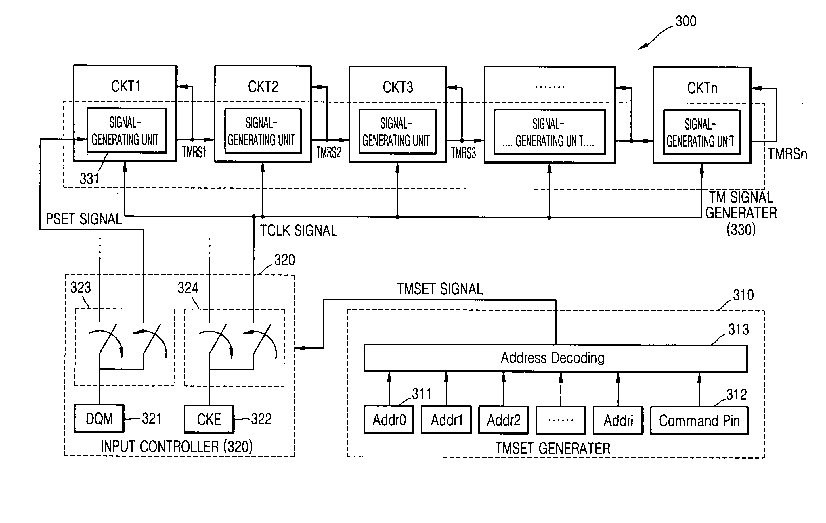
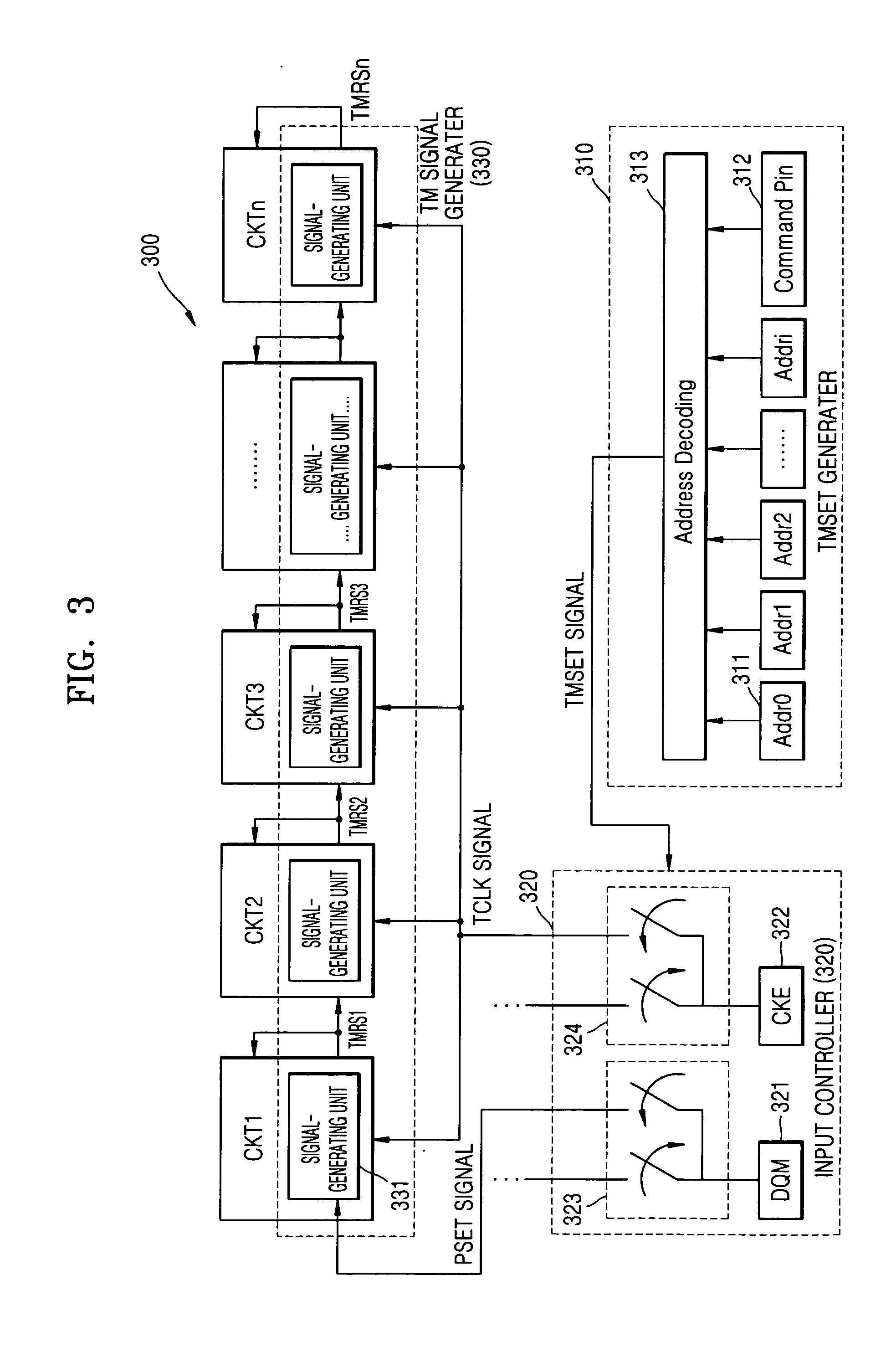
[0027]FIG. 3 is a block diagram of a test-mode signal generating circuit 300 in a memory device according to an embodiment of the present invention. Referring to FIG. 3, the test-mode signal generating circuit 300 includes a test mode entry signal (TMSET signal) generator 310, an input controller 320, and a test mode (TM) signal generator 330.

[0028] The TMSET signal generator 310 includes a plurality of address input units 311 (Addr1, Addr1, Addr2, . . . , and Addri), a command signal input unit 312, and an address decoding unit 313. The address input units 311 and the command signal input unit 312 are pins of the memory device in one embodiment of the present invention. The address decoding unit 313 generates a TMSET signal in response to address information input through the address input units 311 and a command signal input through the command signal input unit 312.

[0029] In other words, the address decoding unit 313 generates only the TMSET signal, unlike a conventional addres...


PUM


Abstract

A memory device includes a plurality of test mode signal generating units and a plurality of test circuits. Each test mode signal generating unit generates a respective test mode signal for a respective test circuit. The test mode signal generating units generate the test mode signals in series for the test circuits. Each test mode signal generating unit may be disposed within a respective test circuit such that wiring is not necessary from the source of the test mode signals to the test circuits.

Description

BACKGROUND OF THE INVENTION [0001] This application claims priority to Korean Patent Application No. 2004-72472, filed on Sep. 10, 2004, in the Korean Intellectual Property Office, the disclosure of which is incorporated herein in its entirety by reference. [0002] 1. Field of the Invention [0003] The present invention relates generally to memory devices, and more particularly, to generation of test mode signals for testing a memory device with minimized wiring. [0004] 2. Description of the Related Art [0005] Recently, test circuits are included in a memory device to detect defects within the memory devices early so that such defects may be corrected. However, the addition of test circuits to a memory device increases the size of the memory device. The test circuits also require an increase in the number of internal signal buses, thereby further increasing the size of the memory device. [0006] When the memory device is put into a test mode by the test circuits, the memory device stop...

Claims


Application Information

Patent Timeline
IPC IPC(8): G01R31/28G06F11/00
CPCG11C29/46G01R31/31701G11C29/00
Inventor CHANG, YOUNG-UKMOON, GIL-SHINHYUN, DONG-HO
Owner SAMSUNG ELECTRONICS CO LTD
Why Eureka
Try Eureka