Electroluminescence element

a technology of electroluminescence and electroluminescence, which is applied in the direction of discharge tube luminescnet screens, natural mineral layered products, transportation and packaging, etc., can solve the problems of inability to efficiently configure the plurality of emissive layers to efficiently emit light, and the color of the emitted light differs significantly from the reference white color, so as to achieve uniform light emission and improve light emission balance , the effect of easy operation

Inactive Publication Date: 2006-03-30
SANYO ELECTRIC CO LTD
View PDF4 Cites 52 Cited by
  • Summary
  • Abstract
  • Description
  • Claims
  • Application Information

AI Technical Summary

Benefits of technology

[0025] When the above relationships are satisfied, holes and electrons can be injected in each emissive layer so as to achieve uniform light emission easily in an element in which a plurality of emissive layers are provided.
[0026] With the present invention, it is possible to improve the light emission balance among a plurality of layered emissive layers, so that a desired light created by combining desired colors can be achieved, and also so that an element with high efficiency and long life can be easily achieved.

Problems solved by technology

However, some colors, such as white, for example, cannot yet be obtained by a single organic emissive material.
With this method, however, it is not always possible to configure the plurality of emissive layers to efficiently emit light, with the result that the color of the emitted light differs considerably from the reference white color.
Further, while organic EL elements are generally capable of high luminance light emission, a number of unsolved problems remain, including durability of the organic materials used for emissive material, such that the lives of such elements are therefore insufficient.
When a plurality of emissive layers are layered to obtain light of an additive color, the emissive layer with the lowest light emission efficiency or the emissive layer with a large injection current will likely deteriorate faster than the other emissive layers.

Method used


Image

  • Electroluminescence element
  • Electroluminescence element
  • Electroluminescence element

Examples


Embodiment Construction

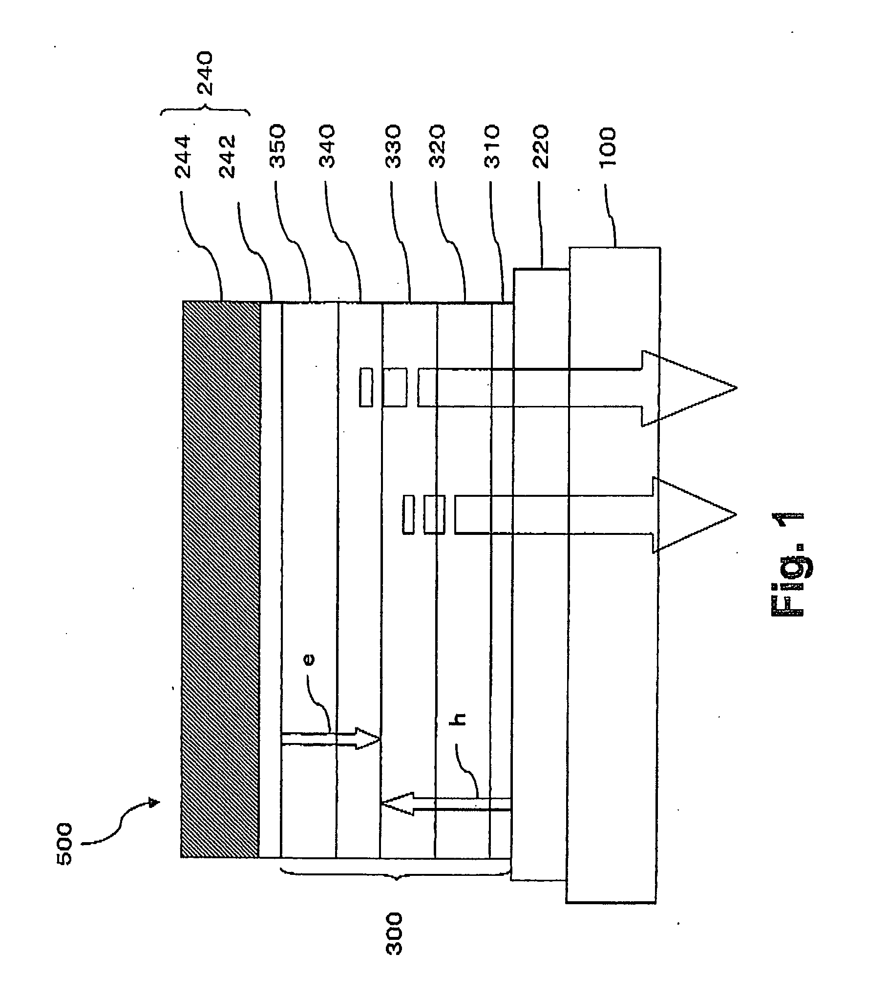
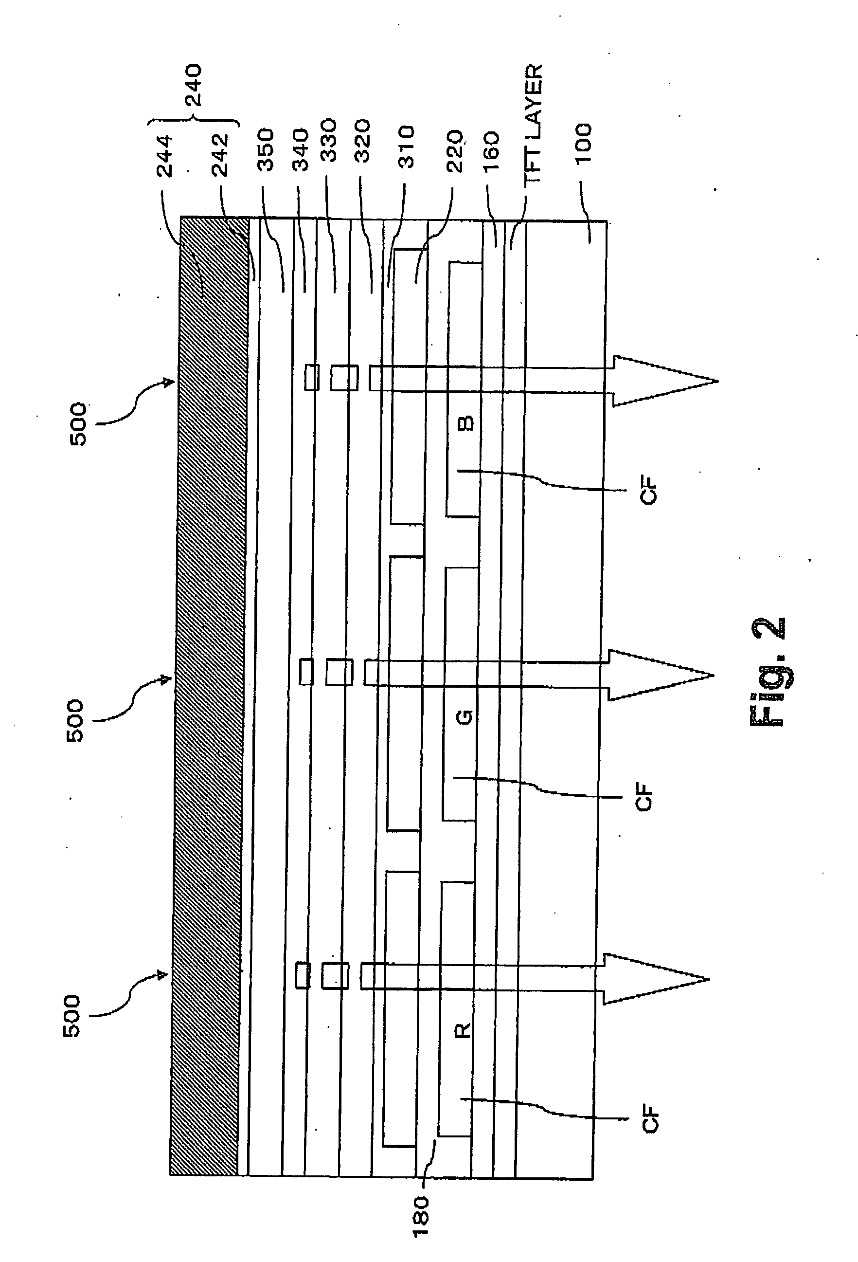
[0033] A preferred embodiment of the present invention will be described in detail with reference to the drawings. FIG. 1 schematically shows a cross sectional structure of an EL element 500 including a plurality of emissive layers between a first electrode and a second electrode according to the preferred embodiment of the present invention.

[0034] One of the first and second electrodes is a hole injecting electrode (anode) 220 and the other is an electron injecting electrode (cathode) 240. In the example shown in FIG. 1, the anode 220 is formed toward a substrate, and the cathode 240 is formed such that the cathode 240 is opposed to the anode 220 with an emissive element layer 300 including an organic compound interposed between these electrodes.

[0035] The emissive element layer 300 includes a plurality of organic layers containing a hole transporting compound. Further, the emissive element layer 300 includes a plurality of emissive layers. The emissive element layer 300 includes...


PUM

PropertyMeasurementUnit
thicknessaaaaaaaaaa
thicknessaaaaaaaaaa
thicknessaaaaaaaaaa

Abstract

An EL element includes, between an anode and a cathode, an emissive element layer including a plurality of emissive layers. The emissive element layer includes two or more organic layers containing a hole transporting compound, and one or more of the plurality of emissive layers contain the hole transporting compound. The concentration of the hole transporting compound in the organic layer which is formed closest to the electron injecting electrode among the organic layers containing the hole transporting compound is lower than the concentration of the hole transporting compound in the organic layer which is formed closest to the hole injecting electrode. When three or more organic layers contain a hole transporting compound, the concentration of the hole transporting compound contained in each organic layer can be set such that, as the organic layer is further away from the hole injecting electrode, the concentration is lower. With this setting, the supply amount and supply timing of holes and electrons can be optimized easily with regard to each of the plurality of emissive layers, so that uniform light emission can be generated in any one of the emissive layers.

Description

CROSS-REFERENCE TO RELATED APPLICATIONS [0001] The entire disclosure of Japanese Patent Applications Nos. 2004-289358 and 2004-289364, including their specifications, claims, drawings, and abstracts, is incorporated herein by reference. BACKGROUND OF THE INVENTION [0002] 1. Field of the Invention [0003] The present invention relates to a structure of an electroluminescence (hereinafter referred to as “EL”) element. [0004] 2. Description of Related Art [0005] In recent years, self-emissive type EL elements have attracted attention as a display element for use in flat panel displays, light sources, and the like. In particular, organic EL elements capable of high brightness light emission in a variety of emission colors depending on the organic compound material employed are being actively studied and developed. [0006] An organic EL element includes an emissive element layer including an emissive layer between a hole injecting electrode (anode) and an electron injecting electrode (cath...

Claims


Application Information

Patent Timeline
Patent Type & Authority Applications(United States)
IPC IPC(8): H01L51/50H05B33/12
CPCH01L27/322H01L51/0059Y10T428/2495H01L51/0081H01L51/5036H01L51/0062H10K59/38H10K85/649H10K85/631H10K85/324H10K50/125H05B33/22H05B33/26
Inventor NISHIKAWA, RYUJISAITO, NOBUO
Owner SANYO ELECTRIC CO LTD
Why Eureka
Try Eureka