Nonvolatile memory cell having floating gate, control gate and separate erase gate, an array of such memory cells, and method of manufacturing

a technology of floating gate and memory cell, which is applied in the direction of semiconductor devices, electrical devices, transistors, etc., can solve the problems of affecting the design of a single member

Inactive Publication Date: 2005-01-20
SILICON STORAGE TECHNOLOGY
View PDF18 Cites 50 Cited by
  • Summary
  • Abstract
  • Description
  • Claims
  • Application Information

AI Technical Summary

Benefits of technology

[0004] Accordingly, in the present invention, a nonvolatile memory cell comprises a substrate of substantially single crystalline semiconductive material having a first conductivity type. A first region of a second conductivity type is in the substrate. A second region of the second conductivity type is in the substrate spaced apart from the first region. A channel region is between the first region and second region with the channel region having a first portion and a second portion. A cont

Problems solved by technology

Secondly, it is supplied with a high voltage during the erase operation to attract the electrons from the spaced apart and i

Method used


Image

  • Nonvolatile memory cell having floating gate, control gate and separate erase gate, an array of such memory cells, and method of manufacturing
  • Nonvolatile memory cell having floating gate, control gate and separate erase gate, an array of such memory cells, and method of manufacturing
  • Nonvolatile memory cell having floating gate, control gate and separate erase gate, an array of such memory cells, and method of manufacturing

Examples


first embodiment

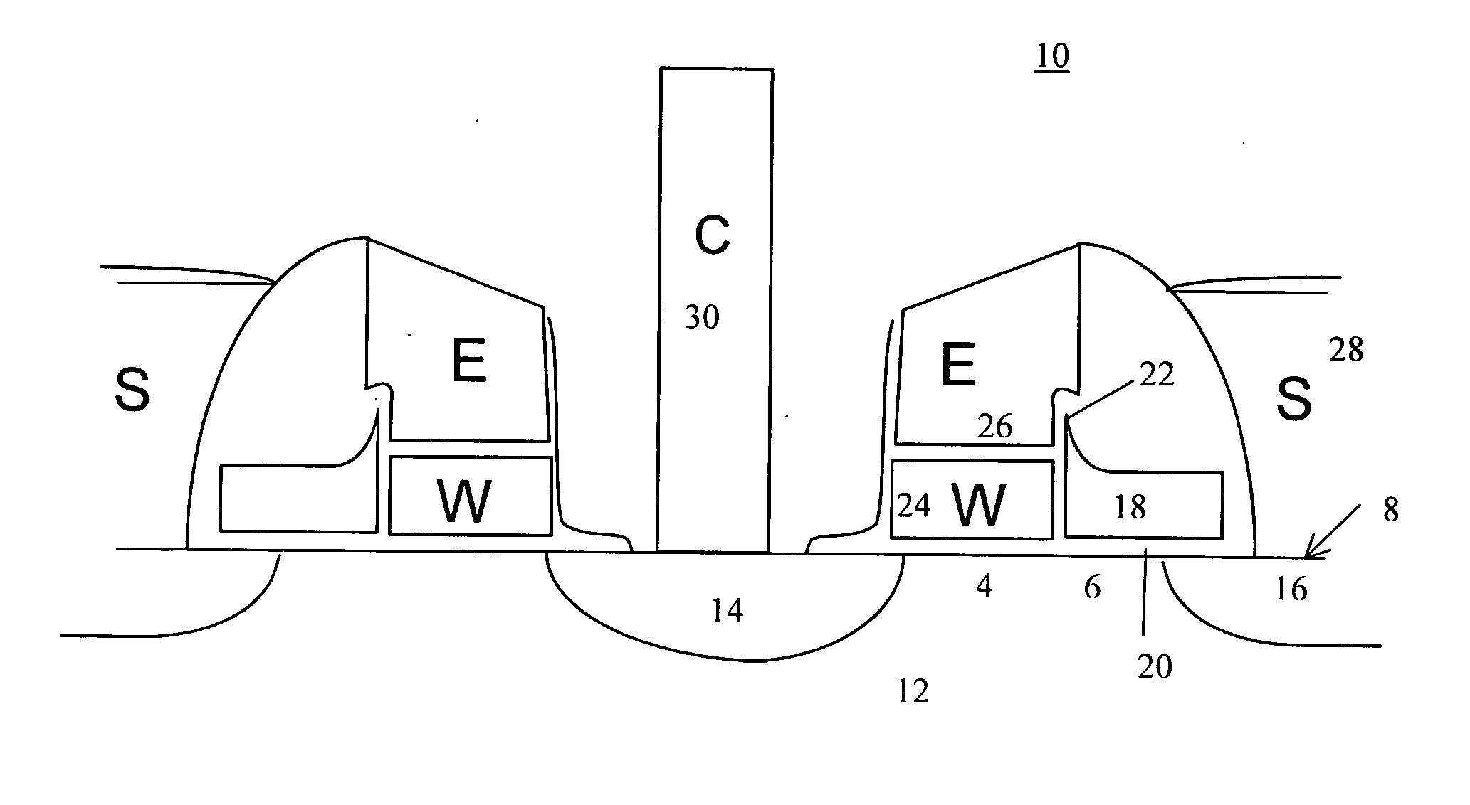
[0011] Referring to FIG. 1A, there is shown a cross-sectional view of a nonvolatile memory cell 10 of the present invention. Similar to the cell shown and described in U.S. Pat. No. 5,029,130, whose disclosure is incorporated herein in its entirety by reference, the memory cell 10 is formed in a substantially single crystalline semiconductor substrate 12, such as silicon. The substrate 12 is of a first conductivity type. The substrate 12 also has a planar surface 8. Within the substrate 12 is a first region 14 of a second conductivity type. A second region 16 of a second conductivity type is spaced apart from the first region 14. Between the first region 14 and the second region 16 is a channel region. The channel region comprises two portions: a first portion 4 which is adjacent to the first region 14 and a second portion 6 which is adjacent to the second region 16. Spaced apart from the substrate 12 is a floating gate 18 which is on a insulating layer 20. The floating gate 18 is p...

second embodiment

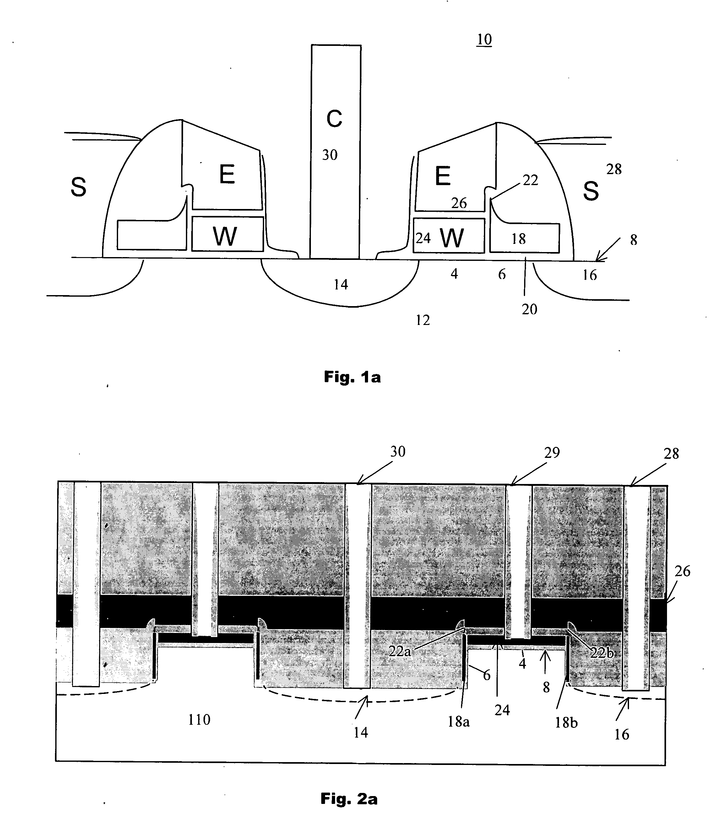
[0025] Referring to FIG. 2A, there is shown a nonvolatile memory cell 110 of the present invention. The cell 110 is similar to the cell 10 shown in FIG. 1A, with the exception that each cell 110 has two floating gates and operates bidirectionally. In addition, the cell 110 has a control gate 24 and a separate erase gate 26 for each cell 110. More specifically, each cell 110 has a first region 14 and a second region 16 spaced apart from one another with a channel region therebetween, in a substrate 12. Each of the first region 14 and a second region 16, however, lies in a trench in the substrate 12 with a portion of the channel region being a planar surface 8. Each of the trenches has a bottom and a side wall with the first region 14 and the second region 16 being at the bottom of the trench. A first floating gate 18A and a second floating gate 18B are along the side of the sidewalls, spaced apart therefrom and insulated therefrom. Thus, each of the floating gate 18A and 18B controls...


PUM


Abstract

A nonvolatile memory cell having a floating gate for the storage of charges thereon has a control gate and a separate erase gate. The cell is programmed by hot channel electron injection and is erased by poly to poly Fowler-Nordheim tunneling. A method for making an array of unidirectional cells in a planar substrate, as well as an array of bidirectional cells in a substrate having a trench, is disclosed. An array of such cells and a method of making such an array is also disclosed.

Description

TECHNICAL FIELD [0001] The present invention relates to a nonvolatile floating gate memory cell having a control gate and a separate erase gate, an array of such cells, and a method of manufacturing. BACKGROUND OF THE INVENTION [0002] Nonvolatile memory cells have a floating gate for the storage of charges thereon to control the conduction of current in a channel in a substrate of a semiconductive material is well known in the art. See, for example, U.S. Pat. No. 5,029,130 whose disclosure is incorporated herein by reference in its entirety. In U.S. Pat. No. 5,029,130, a split gate nonvolatile memory cell having a floating gate with source side injection and poly to poly tunneling is disclosed. The memory cell has a first region and a second region with a channel region therebetween with the channel region having a first portion and a second portion. A floating gate is disposed over a first portion of the channel region is insulated therefrom and controls the conduction of current i...

Claims


Application Information

Patent Timeline
IPC IPC(8): H01L21/8247H01L27/115H01L29/423H01L29/788
CPCH01L27/115H01L29/7885H01L29/42328H01L27/11521H10B69/00H10B41/30
Inventor LEVI, AMITAYKLINGER, PAVELCHEN, BOMYTRAN, HIEU VANLEE, DANAFRAYER, JACK E.
Owner SILICON STORAGE TECHNOLOGY
Why Eureka
Try Eureka