High voltage GaN-based transistor structure

a transistor and high-voltage technology, applied in the field of high-voltage transistor heterostructure, can solve the problems of reducing the effectiveness of passivation, degrading the performance of hemt, and reducing the efficiency of passivation, so as to improve the performance of gan transistors and increase the effectiveness of surface traps

Active Publication Date: 2006-04-11
QORVO US INC
View PDF32 Cites 52 Cited by
  • Summary
  • Abstract
  • Description
  • Claims
  • Application Information

AI Technical Summary

Benefits of technology

[0006]The present invention relates to a high voltage and high power gallium nitride (GaN) transistor structure. In general, the GaN transistor structure includes a sub-buffer layer that serves to prevent injection of electrons into a substrate during high voltage operation, thereby improving performance of the GaN transistor during high voltage operation. Preferably, the sub-buffer layer is aluminum nitride, and the GaN transistor structure further includes a transitional layer, a GaN buffer layer, and an aluminum gallium nitride Schottky layer.
[0007]The GaN transistor structure may include a GaN termination layer deposited on the Schottky layer. The GaN termination layer may be implemented separately or in combination with the sub-buffer layer. The GaN termination layer serves to protect the Schottky layer from surface reactions, such as oxidation, during fabrication and device operation. In addition, the GaN termination layer serves as a reproducible termination layer, thereby increasing the effectiveness of passivation of surface traps on the surface of the GaN transistor heterostructure.

Problems solved by technology

However, during high voltage / power operation, electrons may gain enough kinetic energy to be injected into the substrate, thereby degrading the performance of the HEMT.
These surface reactions may degrade the performance of the HEMT and also decrease the effectiveness of passivation.

Method used


Image

  • High voltage GaN-based transistor structure
  • High voltage GaN-based transistor structure
  • High voltage GaN-based transistor structure

Examples


Embodiment Construction

[0012]The embodiments set forth below represent the necessary information to enable those skilled in the art to practice the invention and illustrate the best mode of practicing the invention. Upon reading the following description in light of the accompanying drawing figures, those skilled in the art will understand the concepts of the invention and will recognize applications of these concepts not particularly addressed herein. It should be understood that these concepts and applications fall within the scope of the disclosure and the accompanying claims.

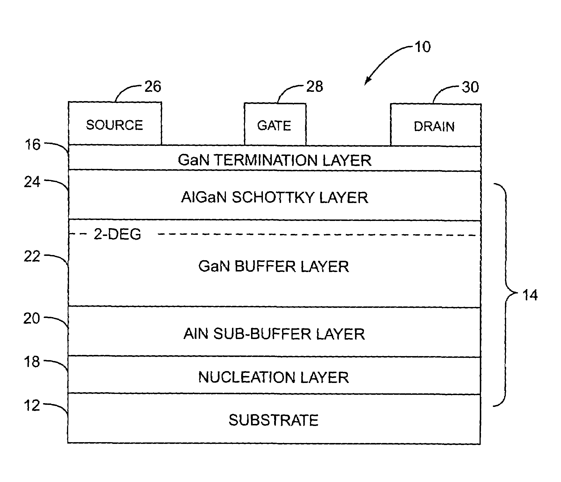
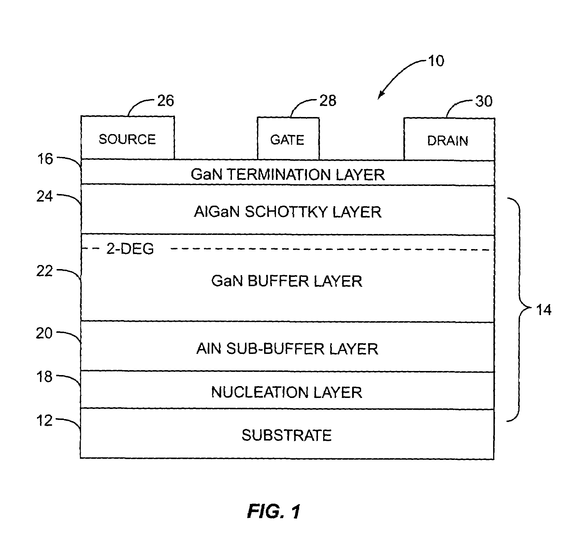
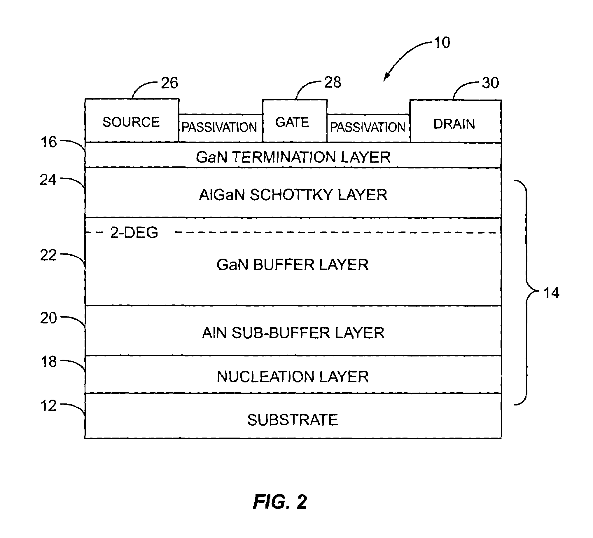
[0013]The present invention relates to a high voltage gallium nitride (GaN) transistor structure preferably incorporated in a high electron mobility transistor (HEMT) 10 as illustrated in FIG. 1. The HEMT 10 includes a substrate 12, structural epitaxial layers 14, and a GaN termination layer 16. The structural epitaxial layers 14 include a nucleation (transitional) layer 18, an aluminum nitride (AlN) sub-buffer layer 20, a GaN buf...


PUM


Abstract

The present invention relates to a high voltage and high power gallium nitride (GaN) transistor structure. In general, the GaN transistor structure includes a sub-buffer layer that serves to prevent injection of electrons into a substrate during high voltage operation, thereby improving performance of the GaN transistor structure during high voltage operation. Preferably, the sub-buffer layer is aluminum nitride, and the GaN transistor structure further includes a transitional layer, a GaN buffer layer, and an aluminum gallium nitride Schottky layer.

Description

[0001]This application claims the benefit of provisional patent application Ser. No. 60 / 503,972, filed Sep. 19, 2003, the disclosure of which is hereby incorporated by reference in its entirety.FIELD OF THE INVENTION[0002]The present invention relates to a high voltage transistor heterostructure, and more particularly relates to a high voltage gallium nitride (GaN) high electron mobility transistor (HEMT).BACKGROUND OF THE INVENTION[0003]Gallium nitride (GaN) offers substantial opportunity to enhance performance of electronic devices such as high electron mobility transistors (HEMTs). In general, a GaN HEMT has a Schottky layer and a GaN buffer layer deposited on a substrate and source, gate, and drain contacts deposited on the Schottky layer. However, during high voltage / power operation, electrons may gain enough kinetic energy to be injected into the substrate, thereby degrading the performance of the HEMT.[0004]In addition, the Schottky layer is typically metallic and may be expo...

Claims


Application Information

Patent Timeline
Patent Type & Authority Patents(United States)
IPC IPC(8): H01L31/072H01L31/109
CPCH01L29/7787H01L29/2003
Inventor SMART, JOSEPHHOSSE, BROOKGIBB, SHAWNGRIDER, DAVIDSHEALY, JEFFREY
Owner QORVO US INC
Why Eureka
Try Eureka