Low forming voltage non-volatile storage device

a non-volatile storage, low-forming voltage technology, applied in semiconductor devices, digital storage, instruments, etc., can solve the problems of high transient current, damage to one or more portions of the memory device, and difficult managemen

Active Publication Date: 2013-07-04
SANDISK TECH LLC
View PDF2 Cites 48 Cited by
  • Summary
  • Abstract
  • Description
  • Claims
  • Application Information

AI Technical Summary

Problems solved by technology

Current FORMING operations often use a high voltage, which can result in high transient currents.
These transient currents make it difficult to manage the FORMING process and sometimes may result in damaging one or more portions of the memory device.
Surge currents are very difficult to control when a resistive memory layer is being formed, especially at higher operational voltage.

Method used


Image

  • Low forming voltage non-volatile storage device
  • Low forming voltage non-volatile storage device
  • Low forming voltage non-volatile storage device

Examples


Embodiment Construction

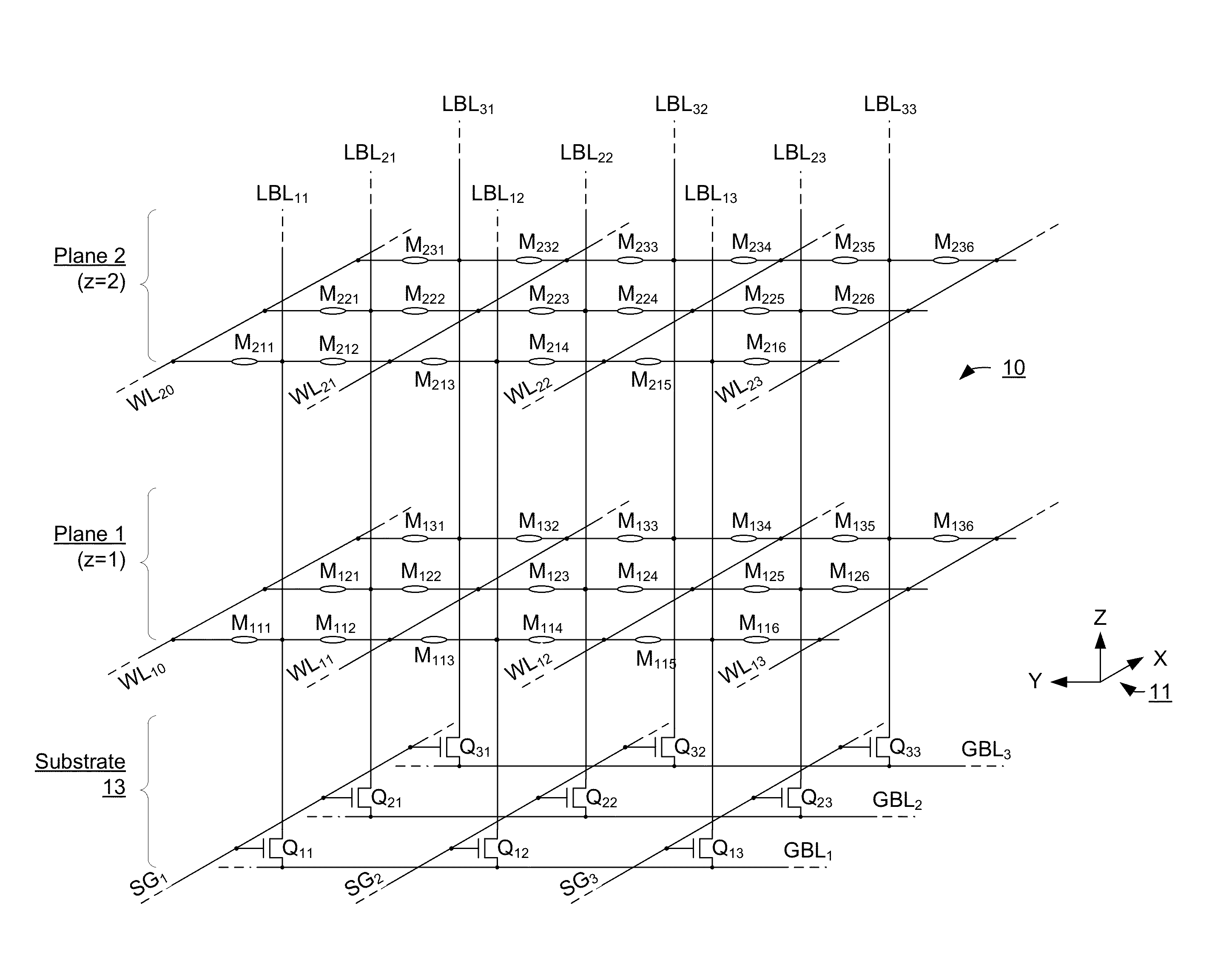
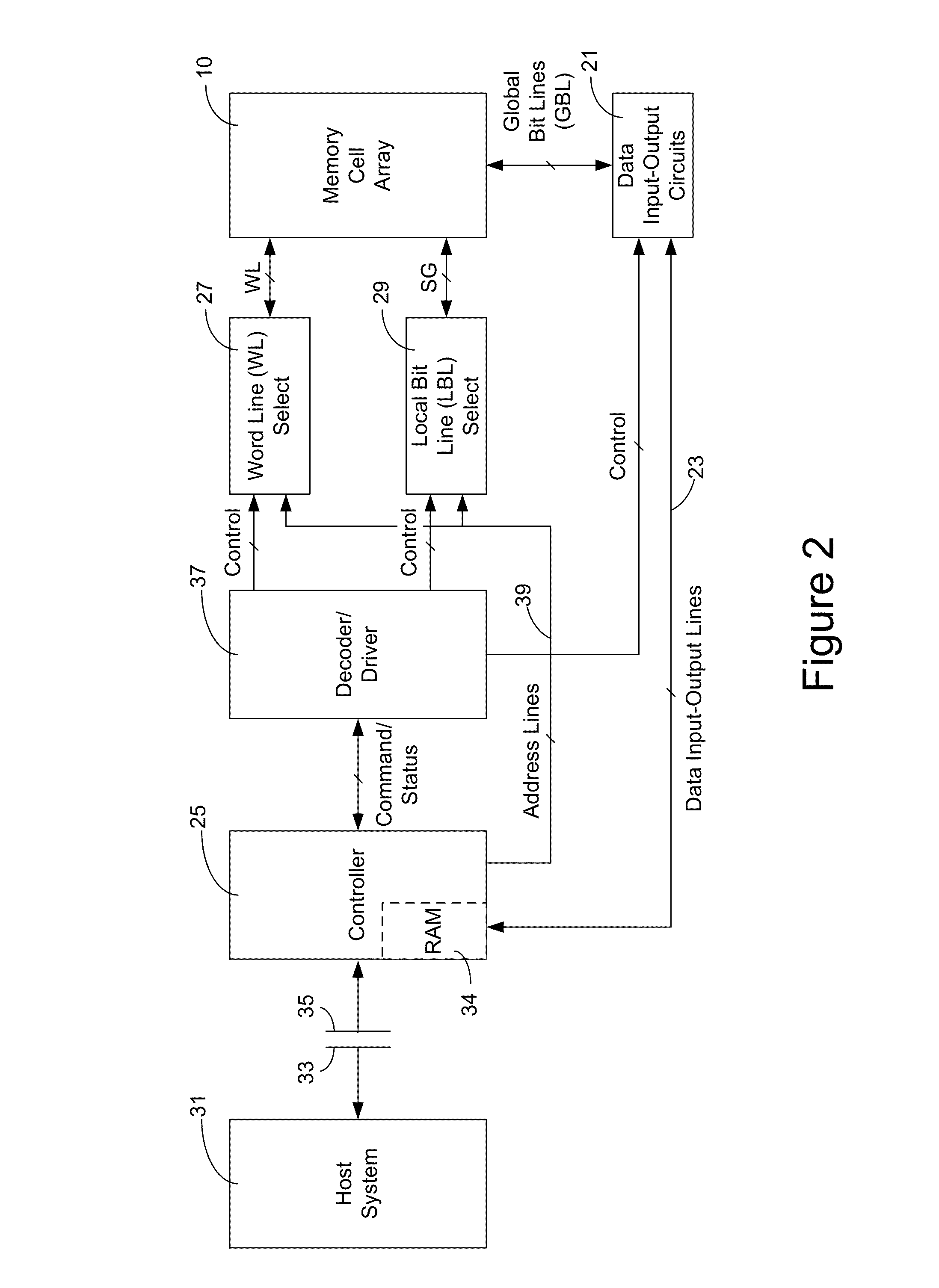
[0035]One embodiment includes a three-dimensional array of memory elements that can be set to a first state and reset to a second state during operation by biasing appropriate voltages on the word lines and bit lines. Prior to operation, the memory elements undergo a forming operation, during which current through the bit lines is limited. A forming voltage is applied to the memory elements during forming with a polarity such that a given bit line acts as a cathode and the appropriate word line acts as an anode, with the cathode having a lower electron injection energy barrier to the switching material than the anode. Such a configuration provides for a more controlled and accurate forming method that does not damage the memory device.

[0036]The memory elements used in the three-dimensional array are preferably variable resistive memory elements. That is, the resistance (and thus inversely the conductance) of the individual memory elements is typically changed as a result of a voltag...


PUM

PropertyMeasurementUnit
currentaaaaaaaaaa
voltageaaaaaaaaaa
voltageaaaaaaaaaa

Abstract

A three-dimensional array of memory elements that reversibly change a level of electrical conductance in response to a voltage difference being applied across them. Memory elements are provided across a plurality of planes positioned different distances above a semiconductor substrate. Bit lines to which the memory elements of all planes are connected are oriented vertically from the substrate and through the plurality of planes. The memory elements can be set to a low resistance state and reset to a high resistance state during standard operation by biasing appropriate voltages on the word lines and bit lines. Prior to standard operation, the memory elements undergo a forming operation, during which current through the bit lines is limited. A forming voltage is applied to the memory elements during forming with a polarity such that the bit line acts as a cathode and the word line acts as an anode, with the cathode having a lower electron injection energy barrier to the switching material than the anode.

Description

[0001]This application claims priority to U.S. Provisional Application 61 / 582,017, filed Dec. 30, 2011, incorporated herein by reference in its entirety.BACKGROUND OF THE INVENTION[0002]1. Field of the Invention[0003]The present invention relates to technology for non-volatile storage.[0004]2. Description of the Related Art[0005]One example of non-volatile memory uses variable resistance memory elements that may be set to either low a low resistance state or a high resistance state, and can remain in that state until subsequently re-set to the initial condition. The variable resistance memory elements are individually connected between two conductors (typically bit and word lines). The state of such a memory element is typically changed by proper voltages being placed on the intersecting conductors.[0006]Some variable resistance memory elements may be in the high resistance state when first fabricated. The term “FORMING” is sometimes used to describe putting the variable resistance ...

Claims


Application Information

Patent Timeline
Patent Type & Authority Applications(United States)
IPC IPC(8): G11C13/00
CPCG11C13/0007H01L27/2454G11C13/0064G11C13/0069H01L45/1253H01L45/146H01L27/249G11C2013/0083G11C2213/32G11C2213/52G11C2213/71G11C2213/77G11C13/0002H01L45/08H01L45/1226H01L45/145G11C13/003H10B63/34H10B63/845H10N70/24H10N70/823H10N70/841H10N70/8833H10N70/883G11C13/004G11C13/0097
Inventor LAN, ZHIDASCHEUERLEIN, ROY E.ZHANG, TONGHOU, KUNRATNAM, PERUMAL
Owner SANDISK TECH LLC
Why Eureka
Try Eureka