

Organic electroluminescent device and manufacturing method thereof
a technology of electroluminescent devices and manufacturing methods, applied in the direction of luminescent screens, discharge tubes, instruments, etc., can solve the problems of unnecessary increase of drive voltage, and achieve the effect of reducing the initial drive voltage and preventing light deterioration
- Summary
- Abstract
- Description
- Claims
- Application Information
AI Technical Summary
Benefits of technology
Problems solved by technology
Method used
Image

Examples
##ventive example 1
Inventive Example 1
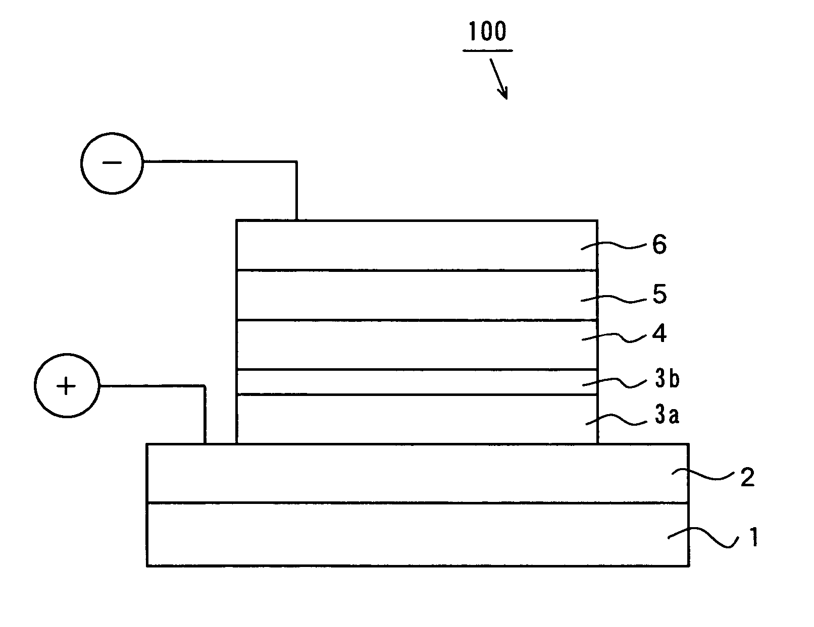
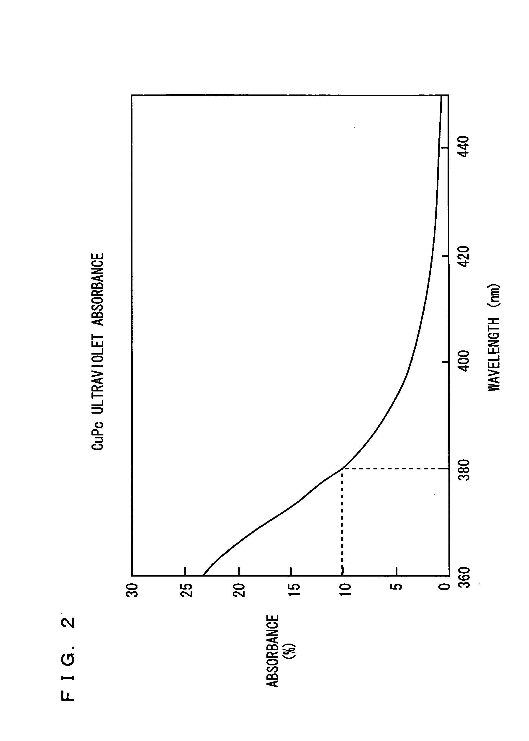
[0050] The organic EL device in Inventive Example 1 was fabricated as follows. A hole injection electrode (anode) 2 made of indium-tin oxide (ITO) was formed on a glass substrate 1, and the glass substrate 1 provided with the hole injection electrode (anode) 2 was cleaned with a neutral detergent, and then subjected to ultrasonic cleaning for ten minutes in acetone and for another ten minutes in ethanol. The surface of the glass substrate 1 was subsequently cleaned by an ozone cleaner. Then, a first hole injection layer 3a made of CuPc was formed on the hole injection electrode (anode) 2 by vacuum evaporation. The first hole injection layer 3a of CuPc has the function of absorbing the ultraviolet light having a wavelength shorter than 380 nm, as mentioned above.
[0051] A second hole injection layer 3b made of CFx was then formed on the first hole injection layer 3a by plasma CVD using CHF3 gas. The second hole injection layer 3b of CFx serves to promote the inject...
##ventive examples 2-8
Inventive Examples 2-8
[0062] Seven types of organic EL devices in Inventive Examples 2 to 8 were fabricated by varying the thicknesses of the first hole injection layers 3a made of CuPc at 0 nm, 3 nm, 5 nm, 10 nm, 15 nm, 17 nm, and 20 nm, respectively. Note that the organic EL devices in Inventive Examples 2 to 8 were fabricated under the same conditions using the same way as in Inventive Example 1.
[0063] Table 2 shows the measurement results of the initial drive voltages and voltage increases after photoirradiation in the organic EL devices in Inventive Examples 2 to 8. FIG. 3 is a graph showing the relationships between the thicknesses of the first hole injection layers 3a of CuPc and the initial drive voltages in the organic EL devices in Inventive Examples 2 to 8. FIG. 4 is a graph showing the relationships between the thicknesses of the first hole injection layers 3a of CuPc and the voltage increases after photoirradiation in the organic EL devices in Inventive Examples 2 to 8...
##ventive examples 9-16
Inventive Examples 9-16
[0070] Eight types of organic EL devices in Inventive Examples 9 to 16 were fabricated by varying the thicknesses of the second hole injection layers 3b of CFx at 0 nm, 0.5 nm, 1 nm, 2 nm, 3 nm, 5 nm, 8 nm, and 10 nm, respectively. Note that the organic EL devices in Inventive Examples 9 to 16 were fabricated under the same conditions using the same way as in Inventive Example 1 except in the thicknesses of the respective second hole injection layers 3b.
[0071] Table 3 shows the measurement results of the initial drive voltages and voltage increases after photoirradiation in the organic EL devices in Inventive Examples 9 to 16. FIG. 5 is a graph showing the relationships between the thicknesses of the second hole injection layers 3b of CFx and the initial drive voltages in the organic EL devices in Inventive Examples 9 to 16. FIG. 6 is a graph showing the relationships between the thicknesses of the second hole injection layers 3b of CFx and the voltage increa...
PUM
| Property | Measurement | Unit |
|---|---|---|
| Fraction | aaaaa | aaaaa |
| Thickness | aaaaa | aaaaa |
| Thickness | aaaaa | aaaaa |
Abstract
Description
Claims
Application Information