Functional film
a technology of functional film and plastic film, applied in the field of functional film, can solve the problems of interlayer peeling between the sealant and the plastic film, deterioration of optical characteristics, etc., and achieve the effect of preventing deterioration of the light emitting elemen
- Summary
- Abstract
- Description
- Claims
- Application Information
AI Technical Summary
Benefits of technology
Problems solved by technology
Method used
Image
Examples
example 1
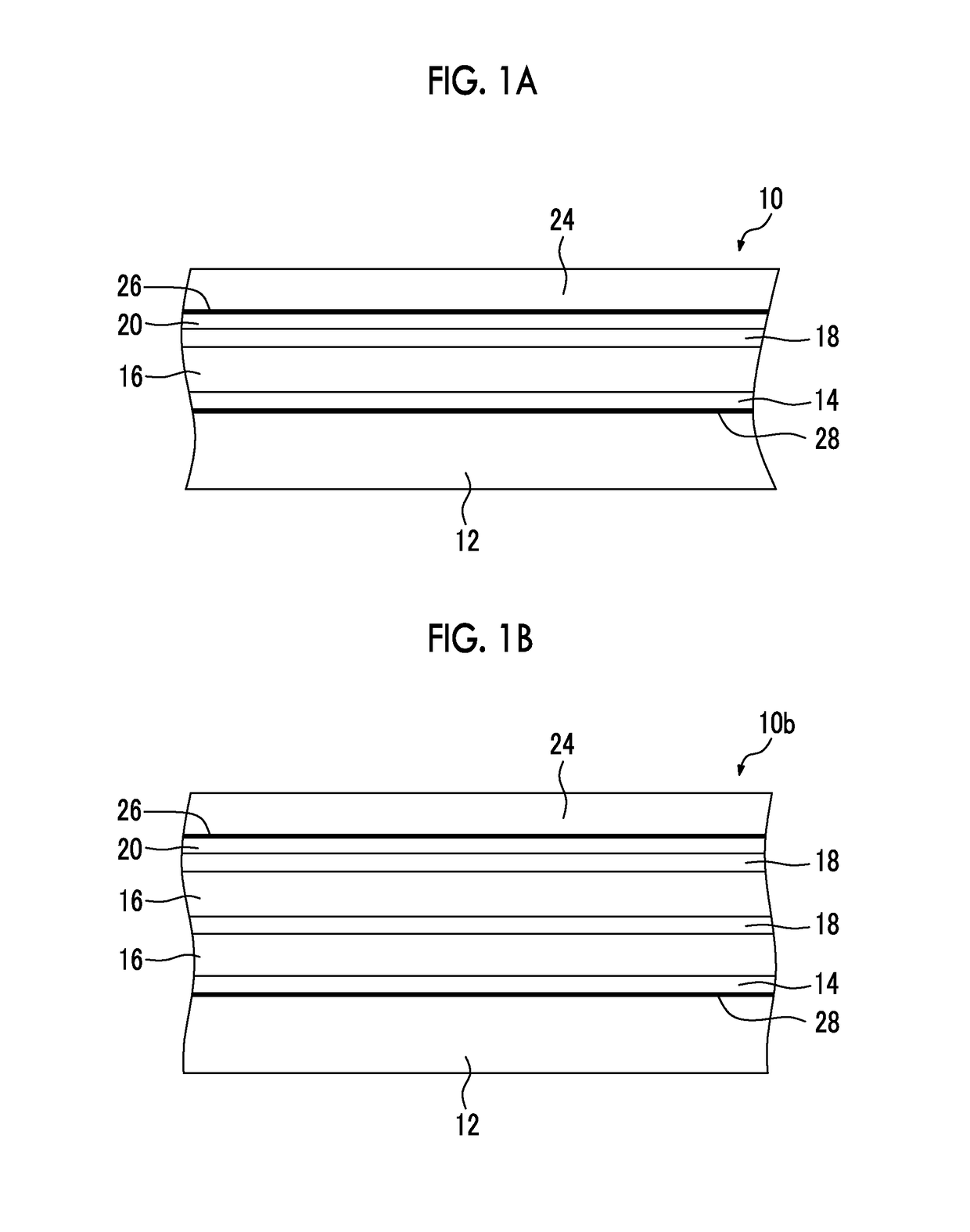
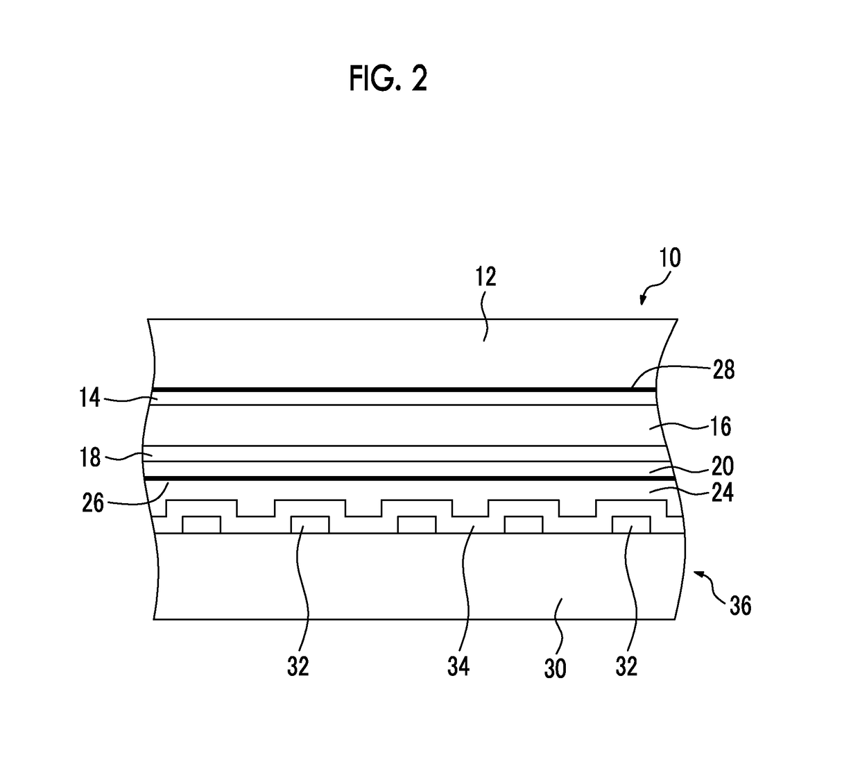
[0177]As the support 12, a COP film (Arton film manufactured by JSR Corporation) having a thickness of 100 μm, a width of 1,000 mm, and a length of 50 m was prepared.
[0178]The support 12 had a value of retardation of 3 nm and Tg of 135° C.
[0179]The support 12 was loaded in a general plasma CVD apparatus, and by plasma CVD (CCP-CVD), the protective inorganic film 14 having a thickness of 25 nm composed of silicon nitride was formed.
[0180]As raw material gases, silane gas (SiH4), ammonia gas (NH3), nitrogen gas (N2), and hydrogen gas (H2) were used. The silane gas was supplied in an amount of 100 sccm, the ammonia gas was supplied in an amount of 200 sccm, the nitrogen gas was supplied in an amount of 500 sccm, and the hydrogen gas was supplied in an amount of 500 sccm. The formation pressure (pressure for forming a film) was 50 Pa.
[0181]For plasma excitation, a power of 3,000 W was supplied at a frequency of 13.56 MHz. During the formation of the film, a bias power of 500 W was suppl...
example 2
[0197]The functional film 10 was prepared in the same manner as in Example 1, except that the bias power was not supplied to the side of the support 12 at the time of forming the protective inorganic film 14.
[0198]A cross section of the functional film 10 was observed in the same manner as in Example 1. As a result, it was verified that although a region, in which the components of the support 12 and the protective inorganic film 14 were mixed together, was observed to be scattered between the support 12 and the protective inorganic film 14, a clear mixed layer 28 was not formed.
example 3
[0199]The functional film 10 was prepared in the same manner as in Example 1, except that a bias power of 300 W was supplied to the side of the support 12 at the time of forming the protective inorganic film 14.
[0200]A cross section of the functional film 10 was observed in the same manner as in Example 1. As a result, it was verified that the mixed layer 28 having a thickness of 10 nm was formed between the support 12 and the protective inorganic film 14.
PUM
| Property | Measurement | Unit |
|---|---|---|
| thickness | aaaaa | aaaaa |
| thickness | aaaaa | aaaaa |
| thickness | aaaaa | aaaaa |
Abstract
Description
Claims
Application Information

