OLED display apparatus with in cell touch structure
a display apparatus and in-cell technology, applied in the field of in-cell touch structure of display apparatus, can solve the problems of easy damage to the touch structure, large thickness, and cell touch panel
- Summary
- Abstract
- Description
- Claims
- Application Information
AI Technical Summary
Benefits of technology
Problems solved by technology
Method used
Image
Examples
first embodiment
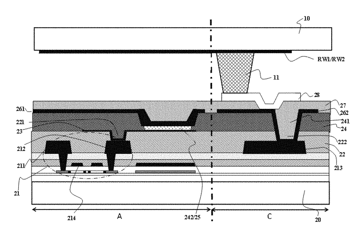
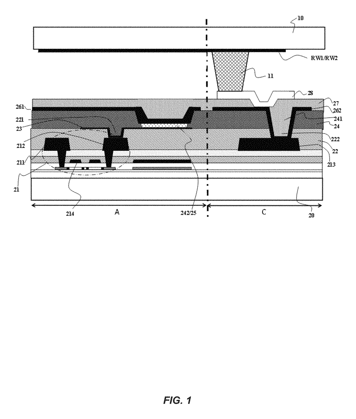
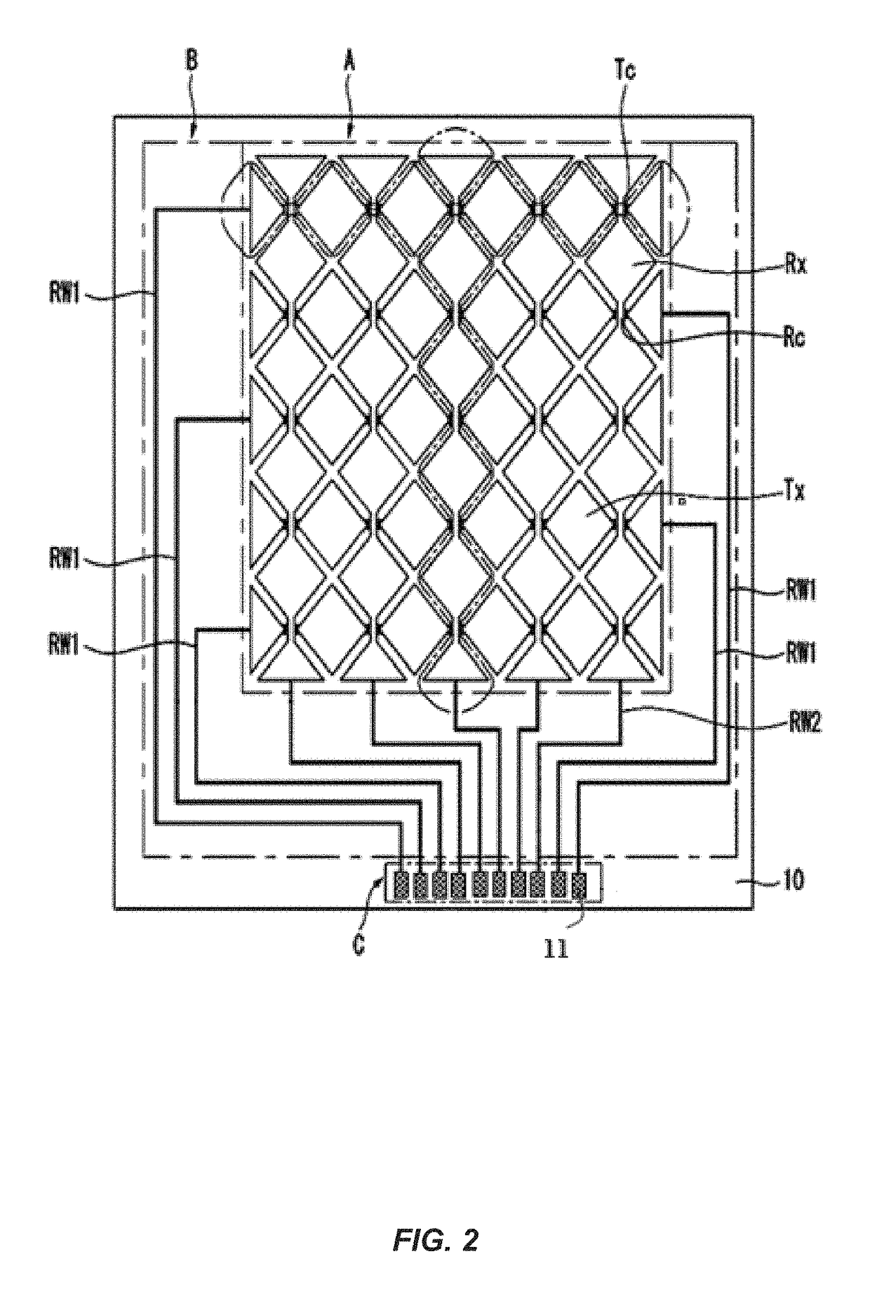
[0020]Multiple driving lines RW1 and multiple sensing lines RW2 are arranged at an inner side of the cover plate 10 facing the array substrate 20. The driving lines RW1 cross the sensing lines RW2 and are insulated from the sensing lines RW2. In the display area A, each of the driving lines RW1 includes multiple driving electrodes Tx arranged in a horizontal direction, and multiple first connecting lines Tc arranged between the adjacent driving electrodes Tx to connect the adjacent driving electrodes Tx. In the display area A, each of the sensing lines RW2 includes multiple sensing electrodes Rx arranged in a vertical direction, and multiple second connecting lines Rc arranged between the adjacent sensing electrodes Rx to connect the adjacent sensing electrodes Rx. In the first embodiment, multiple driving lines RW and multiple sensing lines RW2 constitute a mutual capacitance touch sensing structure. However, in other implementations, multiple driving lines and multiple sensing lin...
second embodiment
[0034]FIG. 6 is a schematic diagram of an OLED display apparatus with an in cell touch structure according to the disclosure. Referring to FIG. 6, the OLED display apparatus with the in cell touch structure includes a cover plate 10, and an array substrate 20 facing the cover plate 10. The OLED display apparatus with the in cell touch structure is divided into a display area A, a layout area B (not shown), and a signal pin area C.
[0035]Multiple driving lines RW1 and multiple sensing lines RW2 are arranged at an inner side of the cover plate 10 facing the array substrate. The driving lines RW1 cross the sensing lines RW2 and are insulated from the sensing lines RW2. In the signal pin area C, multiple driving lines RW1 and multiple sensing lines RW2 are electrically connected to multiple conductive structures 11, respectively. The conductive structures 11 are formed on one side of the cover plate 10, i.e., the conductive structures 11 are formed on the inner side of the cover plate 10...
third embodiment
[0042]FIG. 8 is a cross-sectional view of an OLED display apparatus with an in cell touch structure according to the disclosure. As shown in FIG. 8, the OLED display apparatus with the in cell touch structure includes a cover plate 10 and an array substrate 20 facing the cover plate 10. The OLED display apparatus with the in cell touch structure is divided into a display area A, a layout area B (not shown), and a signal pin area C.
[0043]Multiple driving lines RW1 and multiple sensing lines RW2 are arranged at an inner side of the cover plate 10 facing the array substrate. The driving lines RW1 cross the sensing lines RW2 and are insulated from the sensing lines RW2. The driving lines RW1 and the sensing lines RW2 extend from the display area A up to the signal pin area C.
[0044]At the inner side of the array substrate 20, in the display area A, multiple pixel units are arranged. Each pixel unit includes a thin film transistor 21 and a organic light-emitting layer 25. In the signal pi...
PUM
 Abstract
Description
Claims
Application Information


