
Organic el laminate

Inactive Publication Date: 2015-11-12
FUJIFILM CORP
View PDF8 Cites 3 Cited by
  • Summary
  • Abstract
  • Description
  • Claims
  • Application Information

AI Technical Summary

Benefits of technology

The invention is about a new way to make organic EL devices. If a passivation film and a sealing substrate are used, the device does not need to be sealed with a metal plate or glass, so it can be made lighter and thinner. Using a plastic film instead of glass is even better for making it even lighter and thinner. The invention uses a gas barrier film made of inorganic material to further prevent peeling and deterioration of the device. This new method results in a thinner and lighter organic EL laminate with better protection against moisture and other environmental factors.

Problems solved by technology

However, interlayer peeling, deterioration of the light emitting element caused by the plastic film, and the like occur in some cases.

Method used


Image

  • Organic el laminate
  • Organic el laminate
  • Organic el laminate

Examples


example 1-1

[0163]A 20 mm×20 mm glass plate having a thickness of 500 μm was prepared as the element substrate 20.

[0164]The periphery (2 mm) of the element substrate 20 was masked with ceramic, and the element substrate 20 having undergone masking was loaded in a general vacuum vapor deposition apparatus. By vacuum vapor deposition, an electrode composed of aluminum metal having a thickness of 100 nm was formed, and then a lithium fluoride layer having a thickness of 1 nm was formed.

[0165]On the element substrate 20 on which the electrode and the lithium fluoride layer were formed, the following organic compound layers were sequentially formed by vacuum vapor deposition.

(Light Emitting Layer-Cum-Electron Transport Layer)

[0166]Tris(8-hydroxyquinolinato)aluminum: film thickness of 60 nm

(Second Hole Transport Layer)

[0167]N,N′-diphenyl-N,N′-dinaphthylbenzidine: film thickness of 40 nm

(First Hole Transport Layer)

[0168]Copper phthalocyanine: film thickness of 10 nm

[0169]The element substrate 20 on wh...

example 1-2

[0195]An organic EL laminate was prepared in the same manner as in Example 1, except that the adhesive 16 did not contain a silane coupling agent.

examples 2-1 to 2-5

[0197]Organic EL laminates (Examples 2-1 to 2-5) were prepared in the same manner as in Example 1, except that the thickness of the adhesive 16 of the gas barrier film 14 was changed. Specifically, the thickness of the adhesive 16 of the gas barrier film 14 was changed to 50 μm (Example 2-1), 5 μm (Example 2-2), 2 μm (Example 2-3), 1 μm (Example 2-4), and 300 μm (Example 2-5).


PUM


Abstract

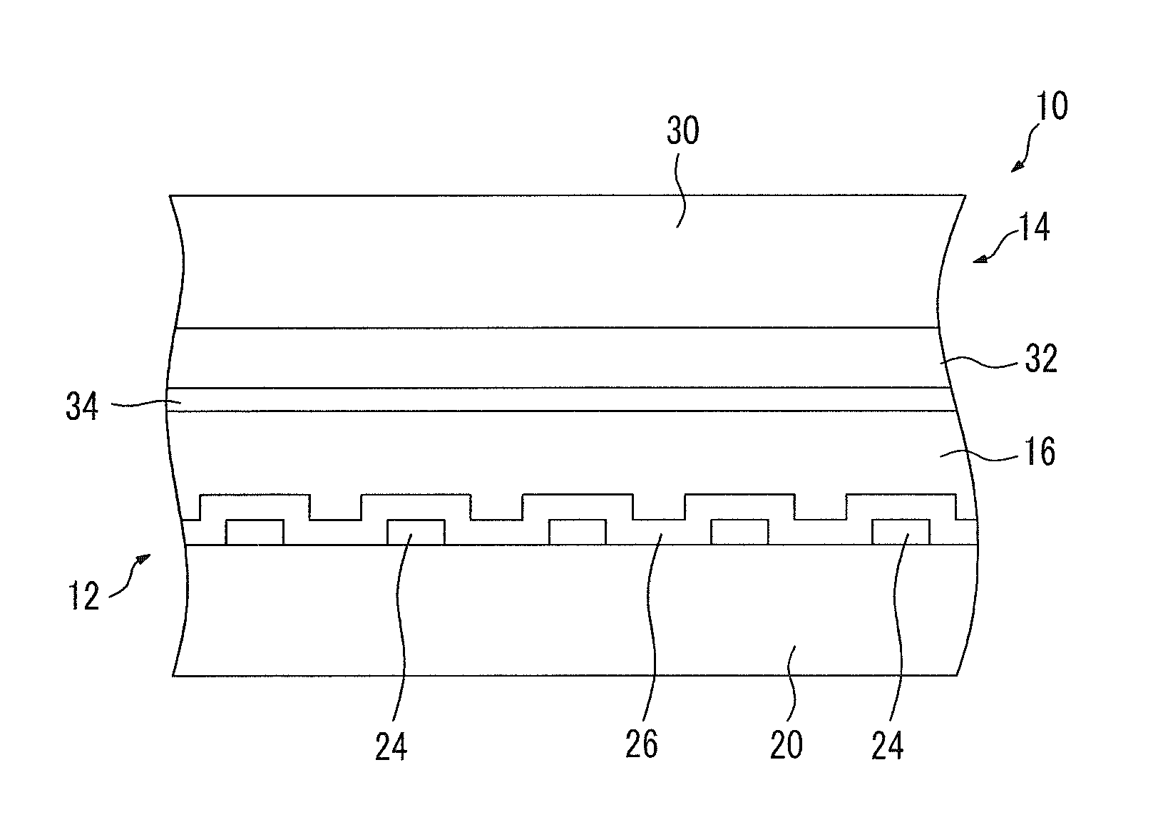
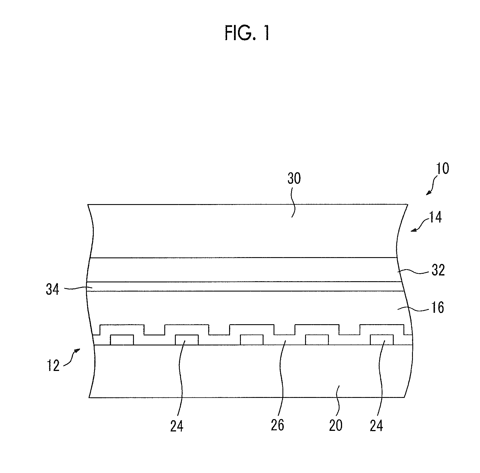
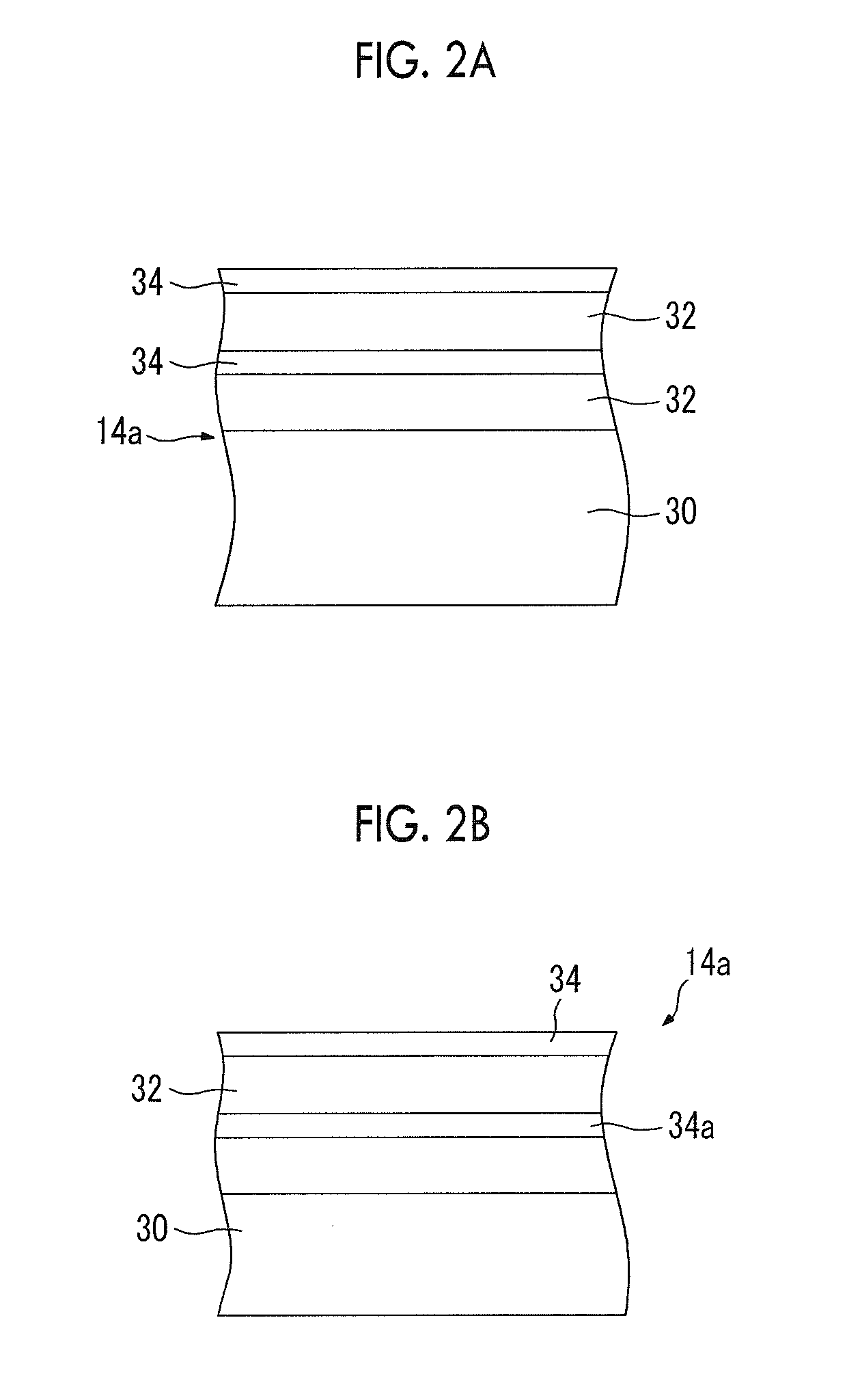
In the organic EL laminate, a gas barrier film, which has a laminated structure composed of an organic film and an inorganic film, adheres to a passivation film, which covers a light emitting element using an organic EL material, by an adhesive in a state in which the inorganic film faces the passivation film and the inorganic film and the passivation film are formed of the same material.

Description

CROSS-REFERENCE TO RELATED APPLICATIONS[0001]This application is a Continuation of PCT International Application No. PCT / JP2014 / 54524, filed on Feb. 25, 2014, which claims priority under 35 U.S.C. §119(a) to Japanese Patent Application No. 2013-046533, filed on Mar. 8, 2013. Each of the above application(s) is hereby expressly incorporated by reference, in its entirety, into the present application.BACKGROUND OF THE INVENTION[0002]1. Field of the Invention[0003]The present invention relates to an organic EL laminate obtained by sealing an organic EL device, in which a light emitting element is protected with a passivation film, with a sealing substrate (gas barrier film).[0004]2. Description of the Related Art[0005]An organic EL device (OLED device) using an organic electro luminescence (EL) material is used in displays, illumination devices, and the like.[0006]The organic EL material used in the organic EL device is extremely vulnerable to moisture. Therefore, for the organic EL de...

Claims


Application Information

Patent Timeline
IPC IPC(8): H01L51/52H01L51/50
CPCH01L51/5253H01L51/5012H01L2251/558H01L2251/303H01L2251/5315H01L51/524H10K59/873H10K59/871H10K50/844H10K50/11H10K50/841H10K2102/00H10K2102/351H10K2102/3026
Inventor IWASE, EIJIRO
Owner FUJIFILM CORP
Learn More