Solid-state image pickup device and fabrication method therefor

a pickup device and solid-state image technology, applied in semiconductor devices, radio frequency controlled devices, electrical devices, etc., can solve the problems of film thickness, deterioration of light blocking performance, etc., to prevent deterioration of light blocking property, reduce wiring line thickness, and enhance the effect of light blocking property

Inactive Publication Date: 2010-08-24
SONY SEMICON SOLUTIONS CORP
View PDF4 Cites 1 Cited by
  • Summary
  • Abstract
  • Description
  • Claims
  • Application Information

AI Technical Summary

Benefits of technology

[0021]Besides, since the third and fourth light blocking films are disposed in a direction perpendicular to the first and second light blocking films, the light blocking property against oblique incident light is enhanced, and a light blocking layer is formed from substantially two metal wiring line layers. Accordingly, the total film thickness of the light blocking film can be increased in comparison with a light blocking film in related art formed from a single metal wiring line layer.
[0051]Further, since the light blocking films are formed with a width with which dishing or erosion does not occur, even if chemical-mechanism polishing is used for formation of the light blocking films, the film thickness of the light blocking films can be assured to a film thickness as designed, and consequently, deterioration of the light blocking property can be prevented.

Problems solved by technology

In short, as enhancement of integration of LSIs advances, also reduction of the film thickness of the light blocking film itself advances and the light blocking performance is deteriorated.
Further, since the film thickness of the light blocking film is reduced by dishing or erosion of CMP used for wiring line working, the light blocking performance is deteriorated.

Method used


Image

  • Solid-state image pickup device and fabrication method therefor
  • Solid-state image pickup device and fabrication method therefor
  • Solid-state image pickup device and fabrication method therefor

Examples


first embodiment

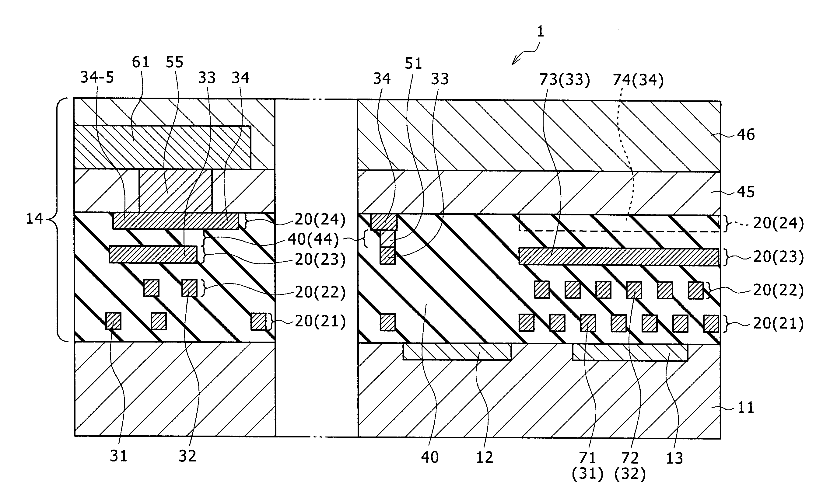
[0067]A first solid-state image pickup device according to the present invention is described with reference to FIGS. 1 and 2. FIG. 1 shows a CMOS image sensor as an example of a solid-state image pickup device.

[0068]Referring first to FIG. 1, the first solid-state image pickup device 1 shown includes a light receiving pixel section 12 and a black level reference pixel section 13 each formed from a photodiode on a semiconductor substrate 11, and a multilayer wiring line section 14 formed on an upper face of the light receiving pixel section 12 and the black level reference pixel section 13.

[0069]The multilayer wiring line section 14 includes a plurality of metal wiring line layers 20 formed in a piled relationship on and in a spaced relationship from each other by a predetermined distance in the thicknesswise direction of the multilayer wiring line section 14 from the semiconductor substrate 11 side. The metal wiring line layers 20 include, for example, a first metal wiring line lay...

second embodiment

[0093]Now, a first solid-state image pickup device according to the present invention is described with reference to FIGS. 3 and 4. FIG. 3 particularly shows a CMOS image sensor as an example of the solid-state image pickup device.

[0094]Referring first to FIG. 3, the first solid-state image pickup device 2 shown includes a light receiving pixel section 12 and a black level reference pixel section 13 each formed from a photodiode on a semiconductor substrate 11, and a multilayer wiring line section 14 formed on an upper face of the light receiving pixel section 12 and the black level reference pixel section 13.

[0095]The multilayer wiring line section 14 includes a plurality of metal wiring line layers 20 formed in a piled relationship on and in a spaced relationship from each other by a predetermined distance in the thicknesswise direction of the multilayer wiring line section 14 from the semiconductor substrate 11 side. The metal wiring line layers 20 include, for example, a first m...

third embodiment

[0123]Now, a second solid-state image pickup device according to the present invention is described with reference to FIGS. 7 and 8. FIG. 7 particularly shows a CMOS image sensor as an example of the solid-state image pickup device.

[0124]Referring first to FIG. 7, the second solid-state image pickup device 3 shown includes a light receiving pixel section 12 and a black level reference pixel section 13 each formed from a photodiode on a semiconductor substrate 11, and a multilayer wiring line section 14 formed on an upper face of the light receiving pixel section 12 and the black level reference pixel section 13.

[0125]The multilayer wiring line section 14 includes a plurality of metal wiring line layers 20 formed in a piled relationship on and in a spaced relationship from each other by a predetermined distance in the thicknesswise direction of the multilayer wiring line section 14 from the semiconductor substrate 11 side. The metal wiring line layers 20 include, for example, a first...


PUM


Abstract

Disclosed herein is a solid-state image pickup device, including, a light receiving pixel section, a black level reference pixel section, a multi-layer wiring line section, a first light blocking film, a second light blocking film, a third light blocking film, and a fourth light blocking layer.

Description

CROSS REFERENCES TO RELATED APPLICATIONS[0001]The present invention contains subject matter related to Japanese Patent Applications JP 2008-231782 and 2008-007730 filed in the Japan Patent Office on Sep. 10, 2008 and Jan. 17, 2008, the entire contents of which being incorporated herein by reference.BACKGROUND OF THE INVENTION[0002]1. Field of the Invention[0003]This invention relates to a solid-state image pickup device and a fabrication method therefor.[0004]2. Description of the Related Art[0005]In a solid-state image pickup device of the CMOS (Complementary Metal Oxide Semiconductor) type which is one of an image sensor, a region into which light should not be admitted, for example, a region of a black level reference pixel section configured to define the block color to be used as a color reference or a peripheral circuit, is normally shielded from light using a metal wiring line or an optical filter. For example, as a light blocking film formed from a metal wiring line, a wirin...

Claims


Application Information

Patent Timeline
Patent Type & Authority Patents(United States)
IPC IPC(8): H01L31/0328
CPCH01L27/1464H01L27/14623H01L27/14609H01L27/14636H01L27/146
Inventor KOBAYASHI, YUSAKUWATANABE, KOJIHAYASHI, TOSHIHIKO
Owner SONY SEMICON SOLUTIONS CORP
Why Eureka
Try Eureka