Apparatus for induced capacitor

a capacitor and induced technology, applied in the field of induced capacitors, can solve the problems of unipolar potentials generated on touch keys, deficient design of touch keys, and possibly not being charged uniformly, and achieve the effect of convenient adjustment of equivalent capacitance of the sam

Inactive Publication Date: 2006-03-30
HOLTEK SEMICON
View PDF7 Cites 53 Cited by
  • Summary
  • Abstract
  • Description
  • Claims
  • Application Information

AI Technical Summary

Benefits of technology

[0006] It is, therefore, an object of the present invention is to provide a capacitive sensing device capable of conveniently adjusting the equivalent capacitance of the same while the area of the device is maintained unchanged.
[0007] It is another object to provide an apparatus for induced capacitor capable of conveniently adjusting the equivalent capacitance of each capacitance sensing devices arranged therein while the overall area of the plural capacitance sensing devices arranged therein is being maintained unchanged.

Problems solved by technology

However, the touch keys are possibly not being charged uniformly due to several factors associated therewith, for example, amount of the touch keys arranged in a touch panel, deficient design of the touch keys and an unevenly formed insulating substrate.
In these cases, the potentials generated on the touch keys are not identical (not uniform).
However, if the equivalent capacitance is increased by enlarging the area, the complexity of designing the touch keys as well as the cost of producing the same may increase since the touch keys may have different shapes and dimensions, and if the equivalent capacitance is increased by reducing the separation between wires, the electric fields induced by the equivalent capacitances in the touch keys reduces correspondingly, which causes the touch keys to have poor sensitivity and functionality.

Method used


Image

  • Apparatus for induced capacitor
  • Apparatus for induced capacitor
  • Apparatus for induced capacitor

Examples


Embodiment Construction

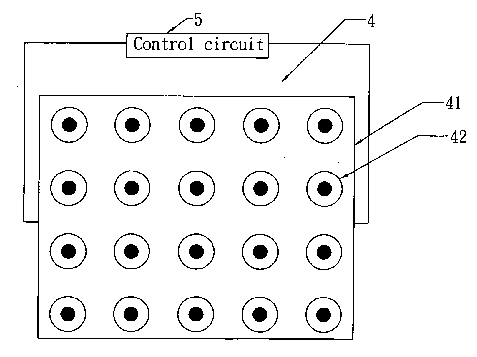
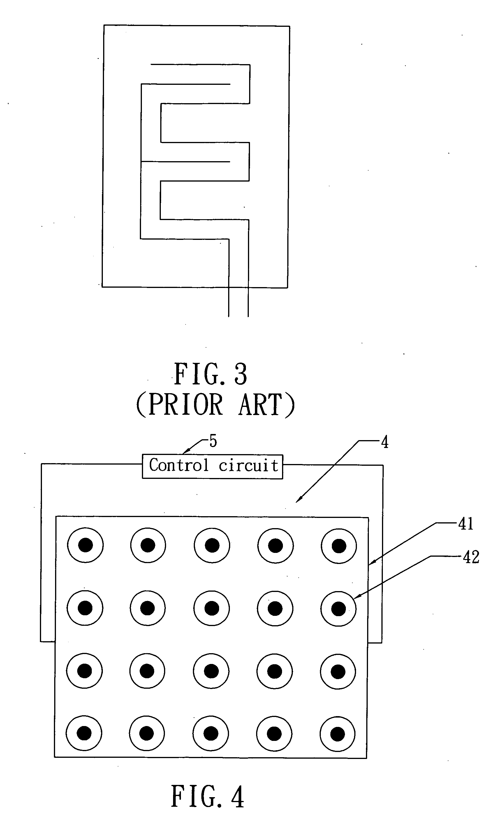
[0017] Pleas refer to FIG. 4, which is is a schematic circuit block diagram showing an apparatus for induced capacitor according to an embodiment of the present invention. The apparatus for induced capacitor 4 is a capacitive touch panel, comprising an insulating substrate 41 and a plurality of capacitive sensing devices 42.

[0018] The insulating substrate 41 is a circuit board selected from the group consisting of a FR4 circuit board, a circuit membrane and the likes. Each of the capacitive sensing devices 42 is used as a touch key, being independently arranged on the insulating substrate 41 and together forming a matrix form. Referring to FIG. 5, an enlarge view of a capacitive sensing device according to the embodiment of the present invention seen in FIG. 4 is illustrated therein. As shown, each of the capacitive sensing devices 42 further comprises a first electrode 43 and a second electrodes 44.

[0019] In this embodiment, the first electrode 43 is a structure of circular profi...


PUM


Abstract

Disclosed is an apparatus for induced capacitor, an insulating substrate; and a plurality of capacitive sensing devices, being arranged on the insulating substrate in a matrix form, each of the plurality of capacitive sensing devices further comprising: a first electrode; and a second electrode, having an inner rim and an outer rim, being disposed circumferentially surrounding the first electrode while separating the second electrode from first electrode by a distance so as to form an equivalent capacitance therebetween, wherein a potential of each capacitive sensing device formed between the two electrodes is adjusted to be a predetermined value by adjusting the distance between the inner rim of the second electrode and the circumference of the first electrode while keeping the outer rim of the second electrode fixed.

Description

FIELD OF THE INVENTION [0001] The present invention relates to an apparatus for induced capacitor, and more particularly, to an apparatus for induced capacitor capable of conveniently adjusting the equivalent capacitance of capacitance sensing devices arranged therein. BACKGROUND OF THE INVENTION [0002] Generally, there are two types of sensing interfaces used by touch panels, which are capacitive type and resistive type. In the case of the capacitive type, a plurality of capacitive touch keys, serving as a sensing medium, have to be formed uniformly on an insulating substrate, such as FR4 substrate and membrane, etc. [0003] The patterning designs of capacitive touch key commonly available are spiral pattern as shown in FIG. 1, comb-like pattern as shown in FIG. 2, and snail-like pattern as shown in FIG. 3, thereby forming an equivalent capacitance. With this configuration, a pulse may be sent by a control circuit to charge the touch keys of a touch panel so as to produce a potentia...

Claims


Application Information

Patent Timeline
Patent Type & Authority Applications(United States)
IPC IPC(8): G09G5/00
CPCG06F3/0202G06F3/044H03K2017/9613H01H2239/006H03K17/9622H01H2229/064G06F3/0443
Inventor LIN, YI-CHAN
Owner HOLTEK SEMICON
Why Eureka
Try Eureka