Semitransmissive liquid crystal display panel

a liquid crystal display panel and semi-transmissive technology, applied in non-linear optics, instruments, optics, etc., can solve the problems of disclination at the periphery of the pixel, unfavorable pixel insertion, and inability to achieve optimal display, etc., to achieve high auxiliary capacitance, alleviate disclination, and reduce the effect of dislocation

Inactive Publication Date: 2006-03-30
SANYO ELECTRIC CO LTD +1
View PDF13 Cites 12 Cited by
  • Summary
  • Abstract
  • Description
  • Claims
  • Application Information

AI Technical Summary

Benefits of technology

[0042] With this structure, even in an MVA-type semitransmissive liquid crystal display panel, it is possible to secure an auxiliary capacitance electrode in such a way that it occupies the greater part of the reflective portion, and thereby to secure a sufficient auxiliary capacitance. Moreover, it is possible, while securing a high auxiliary capacitance in the reflective portion, to restrict the alignm

Problems solved by technology

Disadvantageously, this results in notably uneven display, and causes disclination due to disturbed alignment of liquid crystal molecules at the periphery of each pixel.
The liquid crystal molecules are, in reality, not inclined in an ideal manner, making it impossible to achieve optimum display.
This result

Method used


Image

  • Semitransmissive liquid crystal display panel
  • Semitransmissive liquid crystal display panel
  • Semitransmissive liquid crystal display panel

Examples


Embodiment Construction

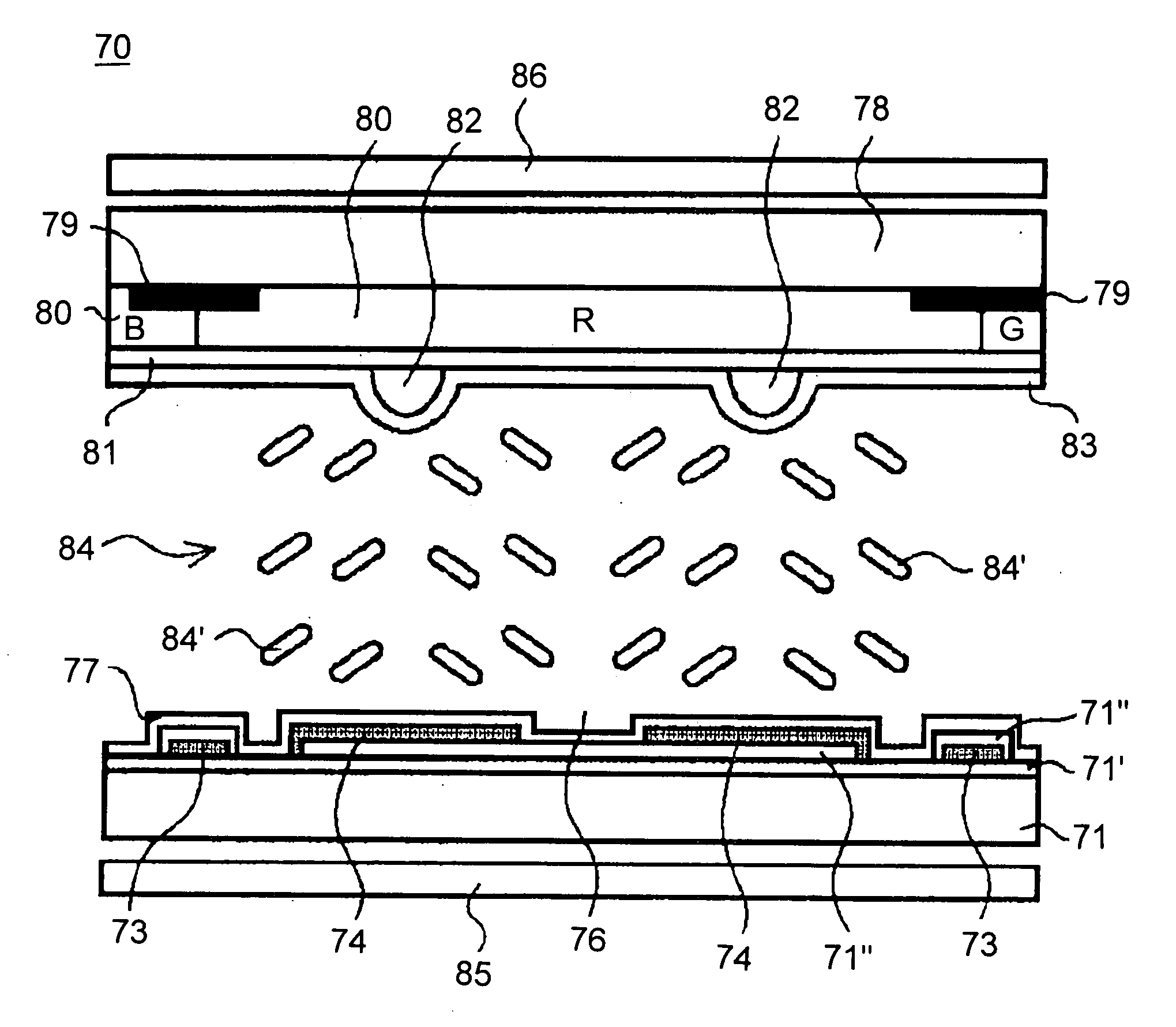
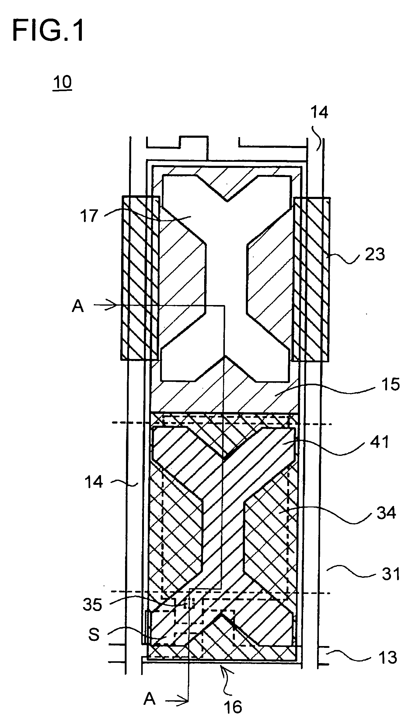
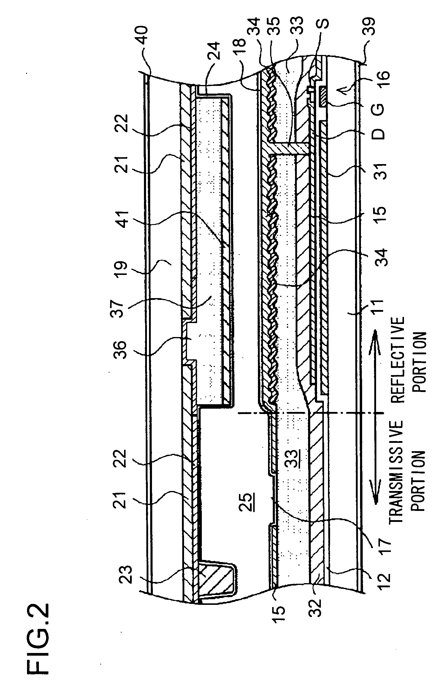
[0052] Hereinafter, embodiments of the present invention will be described with reference to the drawings. The following description deals with semitransmissive liquid crystal display panels as embodiments to which the technical idea of the present invention is applied. It should however be understood that the present invention may be practiced in any manner other than specifically described below. The embodiments described below are directed to small-screen liquid crystal display panels for use in the display section of mobile appliances such as digital cameras and cellular phones, and in particular to those for about 2.2-inch screens with 640×480 pixels (VGA), hence with resolutions of 300 ppi and over, and with 320×240 pixels (QVGA). Accordingly, in these liquid crystal display panels, the size of one pixel is far smaller than in liquid crystal display panels or the like for, for example, 40-inch-screen television monitors.

[0053]FIG. 1 is a plan view schematically showing the pa...


PUM


Abstract

A semitransmissive liquid crystal display panel 10 has a first substrate 11 having, formed in each of the areas demarcated by signal lines and scan lines laid in a grid-like shape thereon, a reflective portion and a transmissive portion formed by a pixel electrode 15 having a slit 17, a second substrate 19 having formed thereon a color filter 21, a common electrode 22, and ridges 23 and 41, alignment films 24 laid over the first and second substrates 11 and 19 and processed for vertical alignment, and a liquid crystal layer 25 laid between the first and second substrates 11 and 19 and showing a negative dielectric constant anisotropy. When no electric field is applied to the liquid crystal layer 25, the liquid crystal molecules are vertically aligned, and, when an electric field is applied to the liquid crystal layer 25, the liquid crystal molecules are horizontally aligned and inclined in the directions restricted by the slit 17 and the ridges 23 and 41. The slit 17 is formed in a central portion of the pixel electrode in the transmissive portion, and the ridges 23 and 41 are formed at the periphery of the pixel electrode 15 and in a central portion of the reflective portion.

Description

[0001] This application is based on Japanese Patent Application No. 2004-289338 filed on Sep. 30, 2004, the contents of which are hereby incorporated by reference. BACKGROUND OF THE INVENTION [0002] 1. Field of the Invention [0003] The present invention relates to a semitransmissive liquid crystal display panel. More particularly, the present invention relates to a semitransmissive liquid crystal display panel of a multi-domain vertical alignment type. [0004] 2. Description of Related Art [0005] Generally, liquid crystal display apparatuses offer the advantages of being slim, lightweight, and power-saving. In particular, TFT (thin-film transistor) liquid crystal display apparatuses are widely used in portable data terminals to large-screen television monitors. One type of liquid crystal display panel for use in liquid crystal display apparatuses is those of a VA (vertical alignment) type. VA-type liquid crystal display panels are widely known to offer fast response combined with a w...

Claims


Application Information

Patent Timeline
IPC IPC(8): G02F1/1337G02F1/1335
CPCG02F1/133707G02F1/1393G02F1/136213G02F1/134336G02F1/1335G02F1/1337G02F1/1343
Inventor TANAKA, SHINICHIRONAKAHARA, TAE
Owner SANYO ELECTRIC CO LTD
Why Eureka
Try Eureka