Pad design for electrochemical mechanical polishing

a technology of mechanical polishing and plating pads, applied in the direction of electrolysis processes, electrolysis components, lapping tools, etc., can solve the problems of excessive conditioning, non-planar feature side of the substrate, and needing planarization

Inactive Publication Date: 2006-04-06
APPLIED MATERIALS INC
View PDF99 Cites 24 Cited by
  • Summary
  • Abstract
  • Description
  • Claims
  • Application Information

AI Technical Summary

Problems solved by technology

As layers of materials are sequentially deposited and removed, the feature side of the substrate may become non-planar and require planarization.
Inherent in this challenge is the difficulty in producing a pad that will not react with process chemistry, which may cause degradation, or require excessive conditioning.
Electrolyte retention in the current conductive pad design becomes difficult when the platen is rotated at higher revolutions per minute (RPM).
This may result in uneven processing or possibly a total cessation of material removal.

Method used


Image

  • Pad design for electrochemical mechanical polishing
  • Pad design for electrochemical mechanical polishing
  • Pad design for electrochemical mechanical polishing

Examples


Embodiment Construction

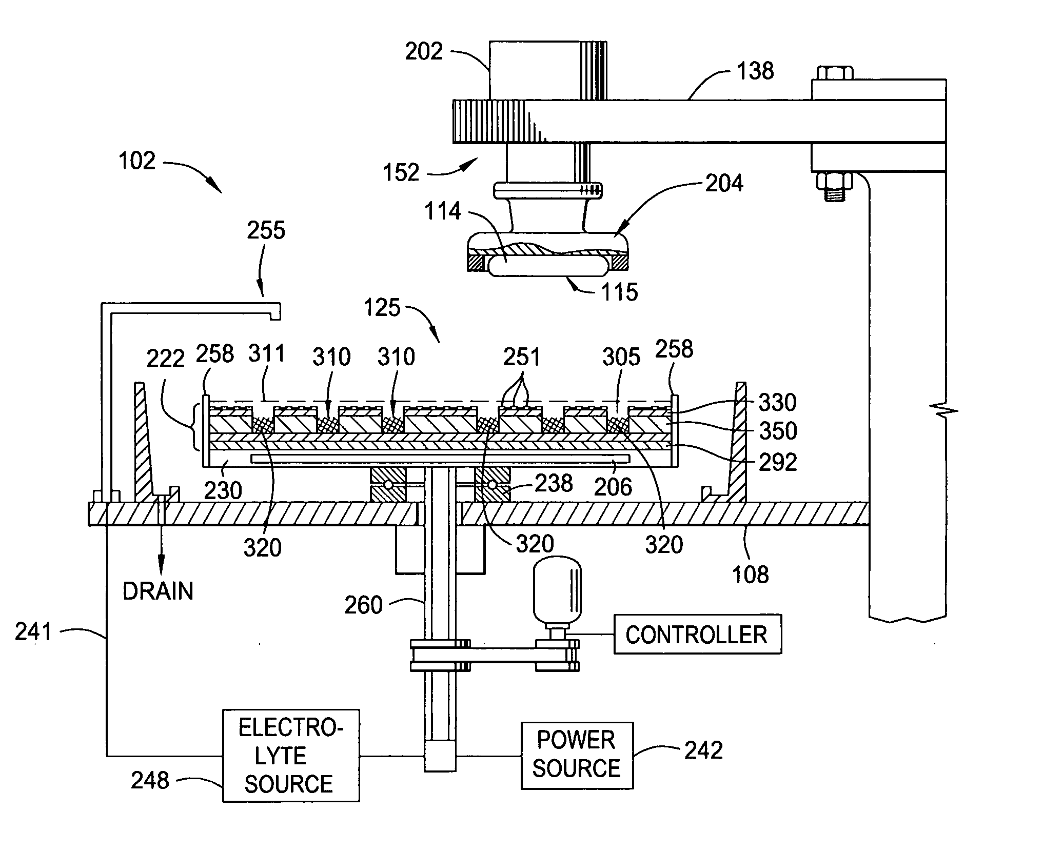
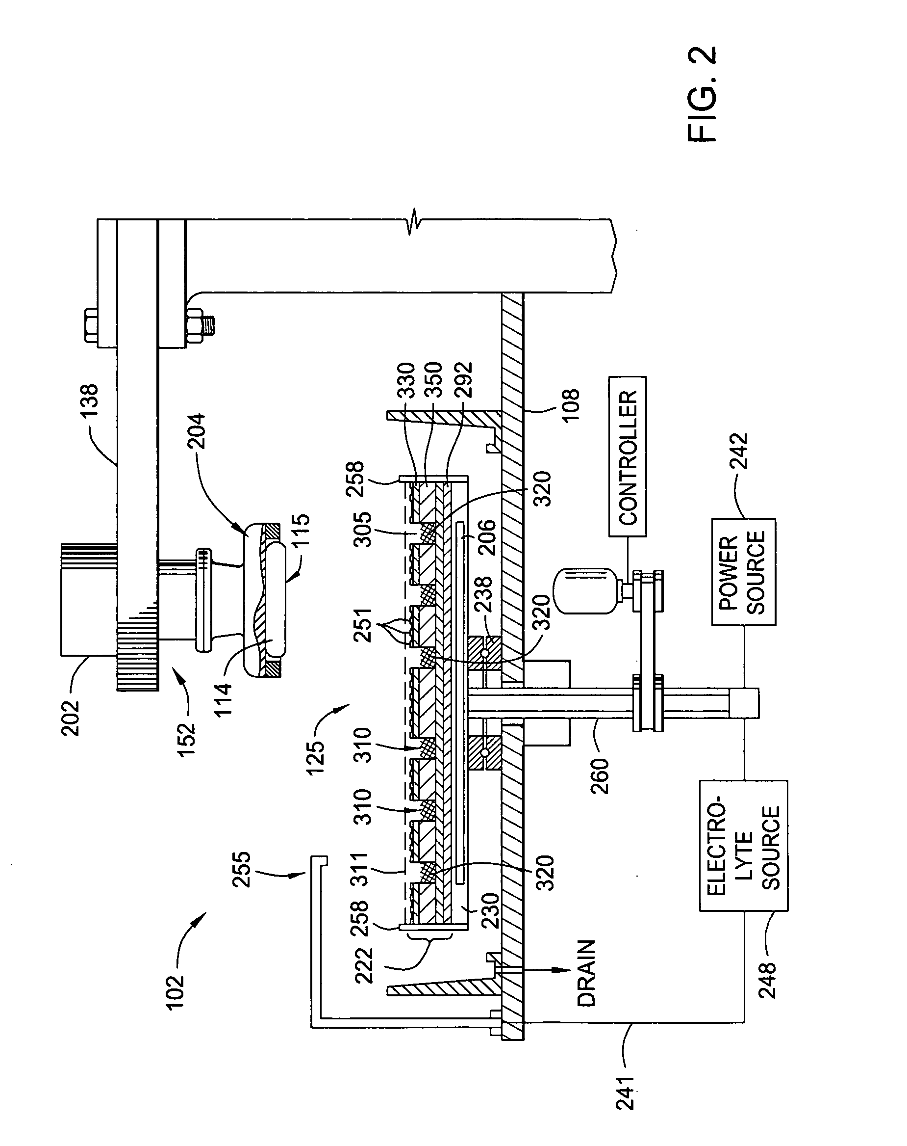
[0027] The words and phrases used in the present invention should be given their ordinary and customary meaning in the art by one skilled in the art unless otherwise further defined. The embodiments described herein may relate to removing material from a substrate, but may be equally effective for electroplating a substrate by adjusting the polarity of an electrical source. Common reference numerals may be used in the Figures, where possible, to denote similar elements depicted in the Figures.

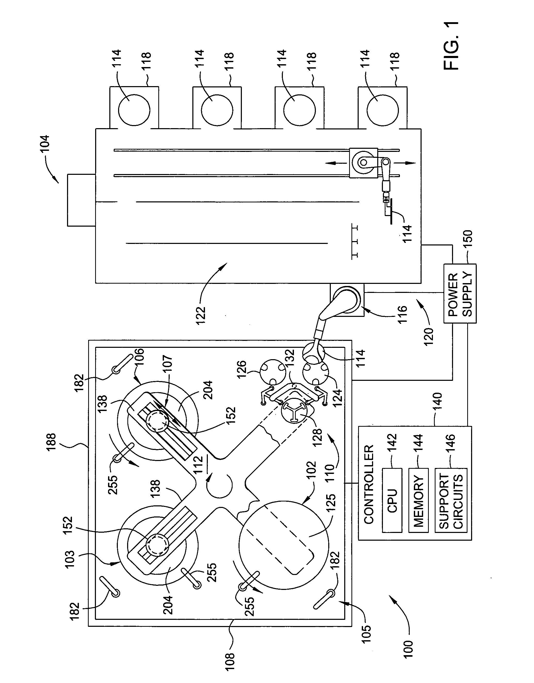
[0028]FIG. 1 is a plan view a processing system 100 having a planarizing module 105 that is suitable for electrochemical mechanical polishing and chemical mechanical polishing. The planarizing module 105 includes at least a first electrochemical mechanical planarization (ECMP) station 102, and optionally, at least one conventional chemical mechanical planarization (CMP) station 106 disposed in an environmentally controlled enclosure 188. An example of a processing system 100 that may be adapte...


PUM

PropertyMeasurementUnit
conductiveaaaaaaaaaa
pressure sensitiveaaaaaaaaaa
thermal sensitiveaaaaaaaaaa

Abstract

A method and apparatus for processing a substrate by electrochemical mechanical planarization and electrochemical mechanical plating is disclosed. Included are various embodiments of a processing pad article comprising an open cell foam subpad that is adapted to retain an electrolyte while encountering centrifugal motion, and simultaneously provide electrical and/or abrasive contact to a feature side of a substrate. Also disclosed is a platen capable of holding an electrolyte during processing at a desired RPM, then releasing the electrolyte centrifugally at a higher RPM. The release is actuated by an operator or by centrifugal force.

Description

CROSS-REFERENCE TO RELATED APPLICATIONS [0001] This application claims benefit of U.S. provisional patent application Ser. No. 60 / 615,198, filed Oct. 1, 2004, which is herein incorporated by reference.BACKGROUND OF THE INVENTION [0002] 1. Field of the Invention [0003] Embodiments of the present invention generally relate to a processing apparatus for planarizing or polishing a substrate. More particularly, the invention relates to polishing pad design for planarizing or polishing a semiconductor wafer by electrochemical mechanical planarization. [0004] 2. Description of the Related Art [0005] In the fabrication of integrated circuits and other electronic devices on substrates, multiple layers of conductive, semiconductive, and dielectric materials are deposited on or removed from a feature side, i.e., a deposit receiving surface, of a substrate. As layers of materials are sequentially deposited and removed, the feature side of the substrate may become non-planar and require planariz...

Claims


Application Information

Patent Timeline
Patent Type & Authority Applications(United States)
IPC IPC(8): C25D17/00B24B37/22
CPCB23H5/08B24B37/22C25F7/00H01L21/32125
Inventor MAVLIEV, RASHID A.BUTTERFIELD, PAUL D.WADENSWEILER, RAPLH M.
Owner APPLIED MATERIALS INC
Why Eureka
Try Eureka