Method and apparatus for determining solder paste composition quality

Inactive Publication Date: 2006-04-06
MV RES
View PDF2 Cites 24 Cited by
  • Summary
  • Abstract
  • Description
  • Claims
  • Application Information

AI Technical Summary

Benefits of technology

[0010] Advantageously the present invention allows for online inspection of substrates, in particular printed circuit boards, having solder paste printed thereon and for determining whether or not the composition of the solder paste is sufficient such that during reflow a sufficient joint can be establishe

Problems solved by technology

In this case the viability of the joint formed with the component may be compromised due to the low metal content in the solder paste.
However, if an incorrect mixture of metal spheres and flux in the solder paste is used as seen with deposit 14 a bad or insufficient joint is established between the component and the deposit.
This ultimately leads to poor electrical contact between the substrate and the component and the incorrect or complete failure of the circuit to which the component b

Method used


Image

  • Method and apparatus for determining solder paste composition quality
  • Method and apparatus for determining solder paste composition quality
  • Method and apparatus for determining solder paste composition quality

Examples


Embodiment Construction

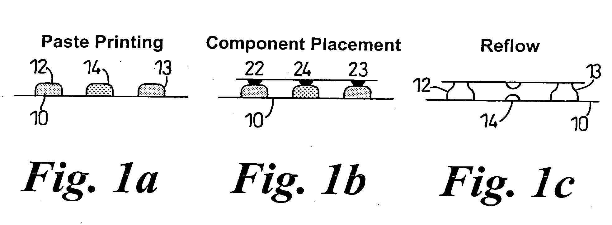
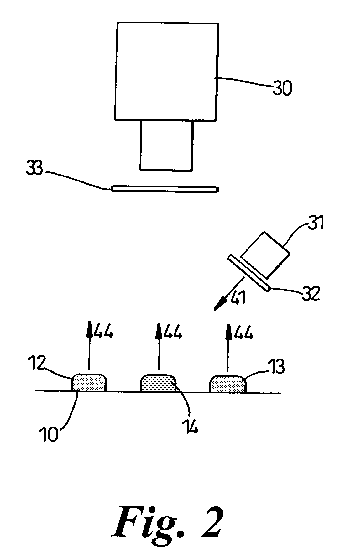
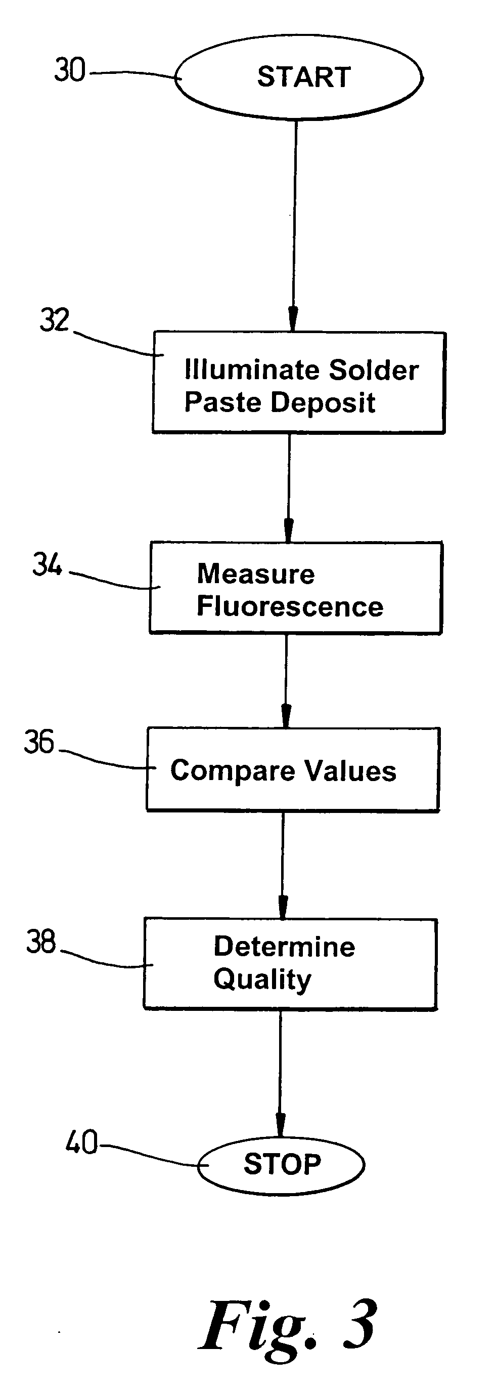
[0017] As can be seen in FIG. 2 where parts also appearing in FIG. 1 bear identical numerical designation, the apparatus of the present invention comprises a light source 31, which is arranged to illuminate deposits 12, 13 and 14 disposed on substrate 10 with radiation 41. The light source for the purposes of this example is a UV light source. The UV light source will typically emit radiation in the 350-400 nm range. A filter 32 is placed in front of the UV light source. The purpose of the filter is to filter out visible light thus ensuring only UV light of the appropriate wavelength (360-380 nm range), typically 370 nm, is incident upon the deposits 12, 13 and 14. The fluorescence will be proportional to the amount of flux present. The UV light source may be comprised of LEDs and may be incorporated in a standard lighting head. The light source may also be arranged in a ring around the deposit in order to improve illumination of the deposit so that the emitted fluorescence radiatio...


PUM

PropertyMeasurementUnit
Nanoscale particle sizeaaaaaaaaaa

Abstract

Determining the quality of a solder paste deposit includes comparing the fluorescence from a solder paste deposit with that of a deposit having an ideal mixture of flux and metal spheres.

Description

CROSS-REFERENCE TO RELATED APPLICATIONS [0001] This application claims priority from British Patent Application No. 0421688.3, filed on Sep. 30, 2004. [0002] The present invention relates to a method for determining solder paste composition. Furthermore the present invention relates to an apparatus for determining the quality of solder paste composition. BACKGROUND [0003] Solder paste is a tacky substance containing small metal spheres typically 15-30 um in diameter, which are held in suspension in an organic viscous fluid commonly known as flux. The paste is sufficiently fluid so as to allow screen-printing onto substrates, such as printed circuit boards (PCB). The printing thickness is typically 80-200 microns and the printed deposits can have areas as low as 0.250 mm2. After printing, components are placed on the substrate with their electrical contacts or pins embedded into the paste. The substrate is then heated beyond the melting temperature of the paste causing the paste to r...

Claims


Application Information

Patent Timeline
IPC IPC(8): B23K31/12G01N21/64H05K1/02H05K3/34
CPCG01N21/6456H05K1/0269H05K3/3484H05K2203/163H05K3/3485
Inventor CONLON, PETERMAHON, JAMES
Owner MV RES
Why Eureka
Try Eureka