Method for flip chip bonding by utilizing an interposer with embedded bumps

Active Publication Date: 2006-04-27
ADVANCED SEMICON ENG INC
View PDF8 Cites 0 Cited by
  • Summary
  • Abstract
  • Description
  • Claims
  • Application Information

AI Technical Summary

Benefits of technology

[0008] One objective of the present invention is to provide a method for flip chip bonding by applying an interposer (such as underfill tape or B-stage material) with embedded bumps to a chip, wherein the bumps do not fill the openings of the interposer completely so as to form a plurality of recessions. When the chip is pressed to a substrate, the pre-solders of the substrate can fill the recessions. As a result, the self-alignment between the bumps and pre-solders in the openings can avoid the sliding movement between the chip and the substrate.

Problems solved by technology

The shortcoming of the conventional method is poor alignment precision.
Therefore, during the pressing procedure, a sliding movement between the chip 10 and the substrate 15 will cause a shift therebetween, which makes the product defective.

Method used


Image

  • Method for flip chip bonding by utilizing an interposer with embedded bumps
  • Method for flip chip bonding by utilizing an interposer with embedded bumps
  • Method for flip chip bonding by utilizing an interposer with embedded bumps

Examples


Embodiment Construction

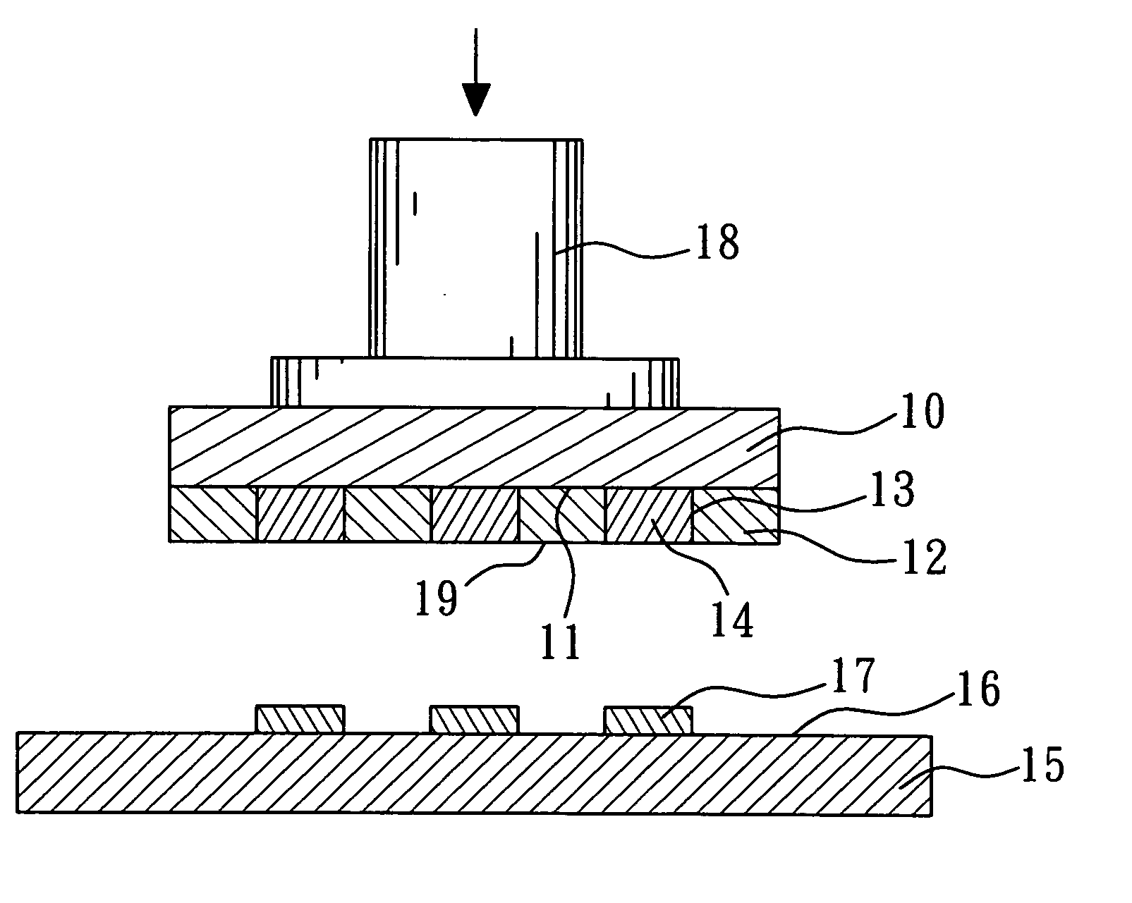
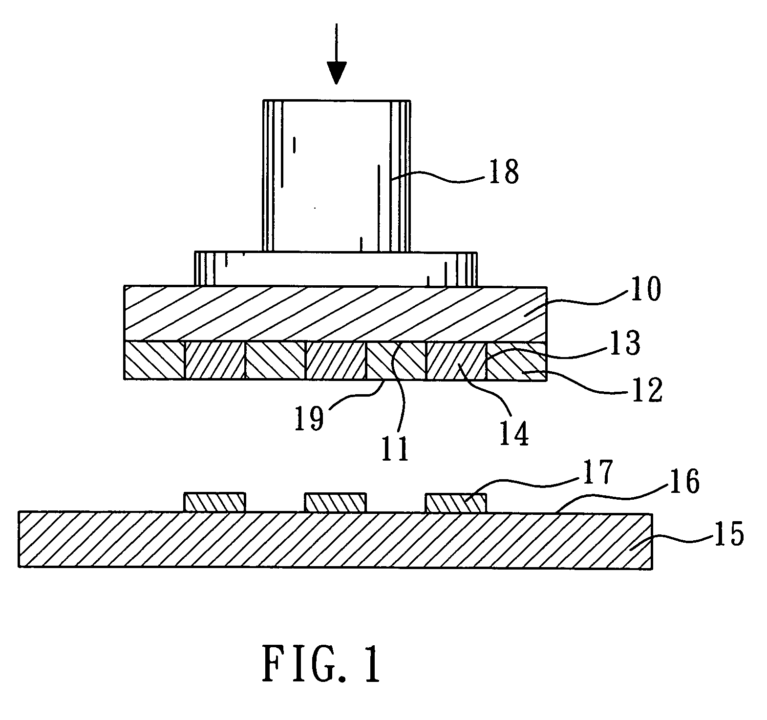
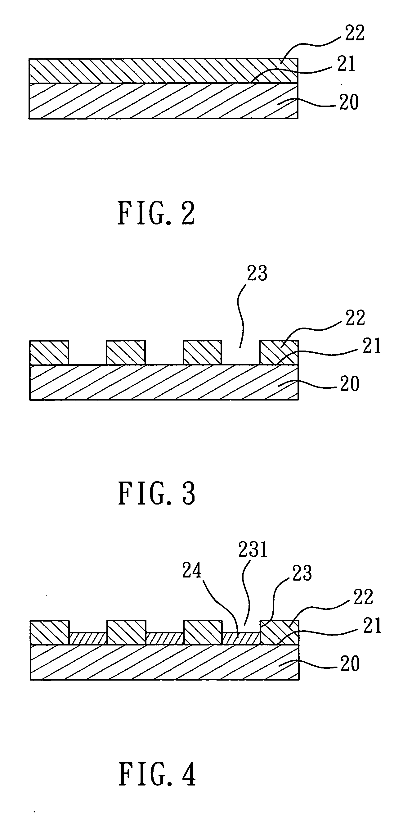
[0018] FIGS. 2 to 6 show a method for flip chip bonding by utilizing an interposer with embedded bumps according to the preferred embodiment of the present invention. The method is described as follows. First, a first element, such as a chip 20, is provided. The chip 20 has a first surface 21. Then, an interposer, such as an underfill tape 22, is adhered to the first surface 21. Then, a plurality of openings 23 are formed on the underfill tape 22 so as to expose the pads (not shown) of the chip 20. The openings 23 may be formed by any conventional method, such as laser drilling, and exposing and developing.

[0019] Then, referring to FIG. 4, a plurality of bumps 24 are formed in the opening 23 by plating. The composition of the bumps 24 is 63% by weight of tin and 37% by weight of lead, or 5% by weight of tin and 95% by weight of lead. Alternatively, the bumps 24 may be gold bumps or copper bumps. The height of the bumps 24 is smaller than the depth of the openings 23 so as to form a...


PUM


Abstract

The present invention relates to a method for flip chip bonding by utilizing an interposer with embedded bumps. The method comprises (a) providing a first element having a first surface; (b) forming an interposer onto the first surface; (c) forming a plurality of openings on the interposer; (d) forming a plurality of bumps in the openings, wherein the height of the bumps is smaller than the depth of the openings; (e) providing a second element having a plurality of pre-solders; and (f) bonding the first surface onto the second element, so that the pre-solders are disposed in the openings and in contact with the bumps. As a result, the self-alignment between the pre-solders and the bumps can avoid the shift between the first element and the second element.

Description

BACKGROUND OF THE INVENTION [0001] 1. Field of the Invention [0002] The present invention relates to a method for flip chip bonding, and more particularly, to a method for flip chip bonding by utilizing an interposer with embedded bumps. [0003] 2. Description of the Related Art [0004]FIG. 1 shows a conventional method for flip chip bonding by utilizing an underfill tape with embedded bumps. The conventional method is described as follows. First, a chip 10 having a chip surface 11 is provided. Then, an underfill tape 12 is adhered to the chip surface 11. Then, a plurality of openings 13 are formed on the underfill tape 12 by laser drilling. Then, a plurality of bumps 14 are formed in the opening 13 by plating, wherein the composition of the bumps 14 is 63% by weight of tin and 37% by weight of lead, and the height of the bump 14 is equal to the depth of the opening 13 so that the bump 14 can fill the opening 13 precisely. [0005] Then, a substrate 15 having a substrate surface 16 is p...

Claims


Application Information

Patent Timeline
IPC IPC(8): H01L21/50H01L21/44H01L21/00H01L21/56H01L21/60H05K3/34
CPCH01L21/563H01L24/16H01L2224/73204H01L2224/32225H01L2924/014H01L2924/01033H01L2924/01006H01L24/29H05K3/3436H01L2924/01082H01L2924/01079H01L2924/01078H01L2924/0105H01L2924/01029H01L2924/01005H01L2224/83856H01L2224/83194H01L2224/83192H01L2224/83191H01L24/81H01L2224/13099H01L2224/13111H01L2224/13144H01L2224/16225H01L2224/73203H01L2224/81801H01L2924/00H01L2924/00014H01L2924/00011H01L2224/0401
Inventor HO, MING-LUNCHUNG, CHIH-MING
Owner ADVANCED SEMICON ENG INC
Why Eureka
Try Eureka