Semiconductor image sensor module, method for manufacturing the same as well as camera and method for manufacturing the same

Inactive Publication Date: 2006-05-04
SONY CORP
View PDF5 Cites 50 Cited by
  • Summary
  • Abstract
  • Description
  • Claims
  • Application Information

AI Technical Summary

Benefits of technology

[0026] According to the embodiment of the semiconductor image sensor module of the present invention, since high-speed signal processing with a minimum-sized module can be performed with the above structure and heat generated by the image signal processing chip can be dissipated through the heat dissipating means, a dark current and white noise to the semiconductor image sensor chip can be prevented from occurring. Since

Problems solved by technology

With the chip-mounted structure of the Patent document 1, since the CCD image sensor 110 of the semiconductor image sensor chip and signal processing chip 116 that is an IC for processing image signals are electrically connected, in which the semiconductor image sensor chip is connected to the image signal processing IC through a contact terminal 111 of the CCD image sensor such as a lead frame, resistance and capacity of the contact terminal need to be considered, which results in interfering with a high-speed image processing.
However, it has been difficult to combine the semiconductor image sensor chip and image signal processing chip, in which a light-receiving surface and an electrode pad are provided on the same surface, by using the above-described SIP t

Method used


Image

  • Semiconductor image sensor module, method for manufacturing the same as well as camera and method for manufacturing the same
  • Semiconductor image sensor module, method for manufacturing the same as well as camera and method for manufacturing the same
  • Semiconductor image sensor module, method for manufacturing the same as well as camera and method for manufacturing the same

Examples


Embodiment Construction

[0039] Hereinafter, embodiments of the present invention will be explained with reference to drawings.

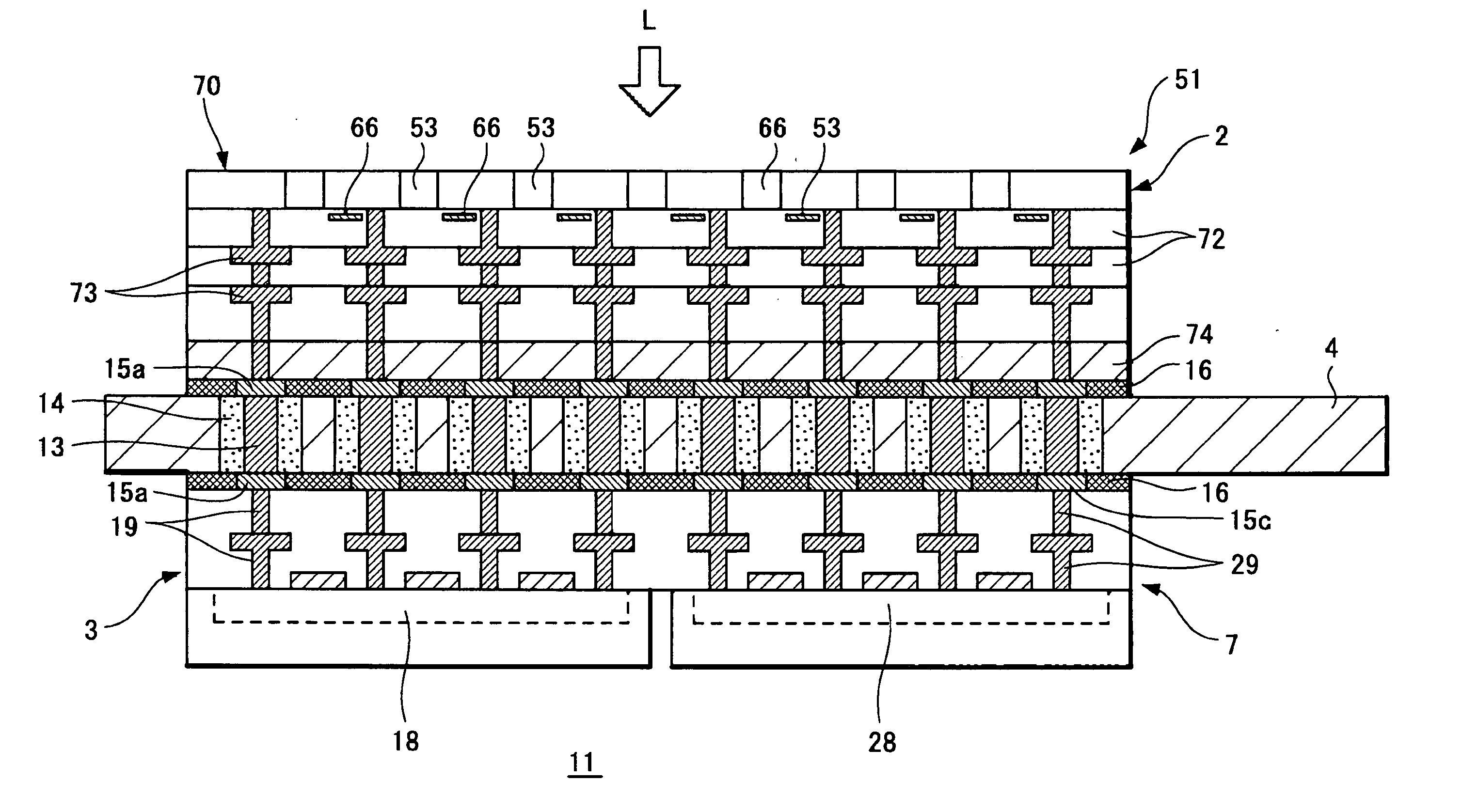
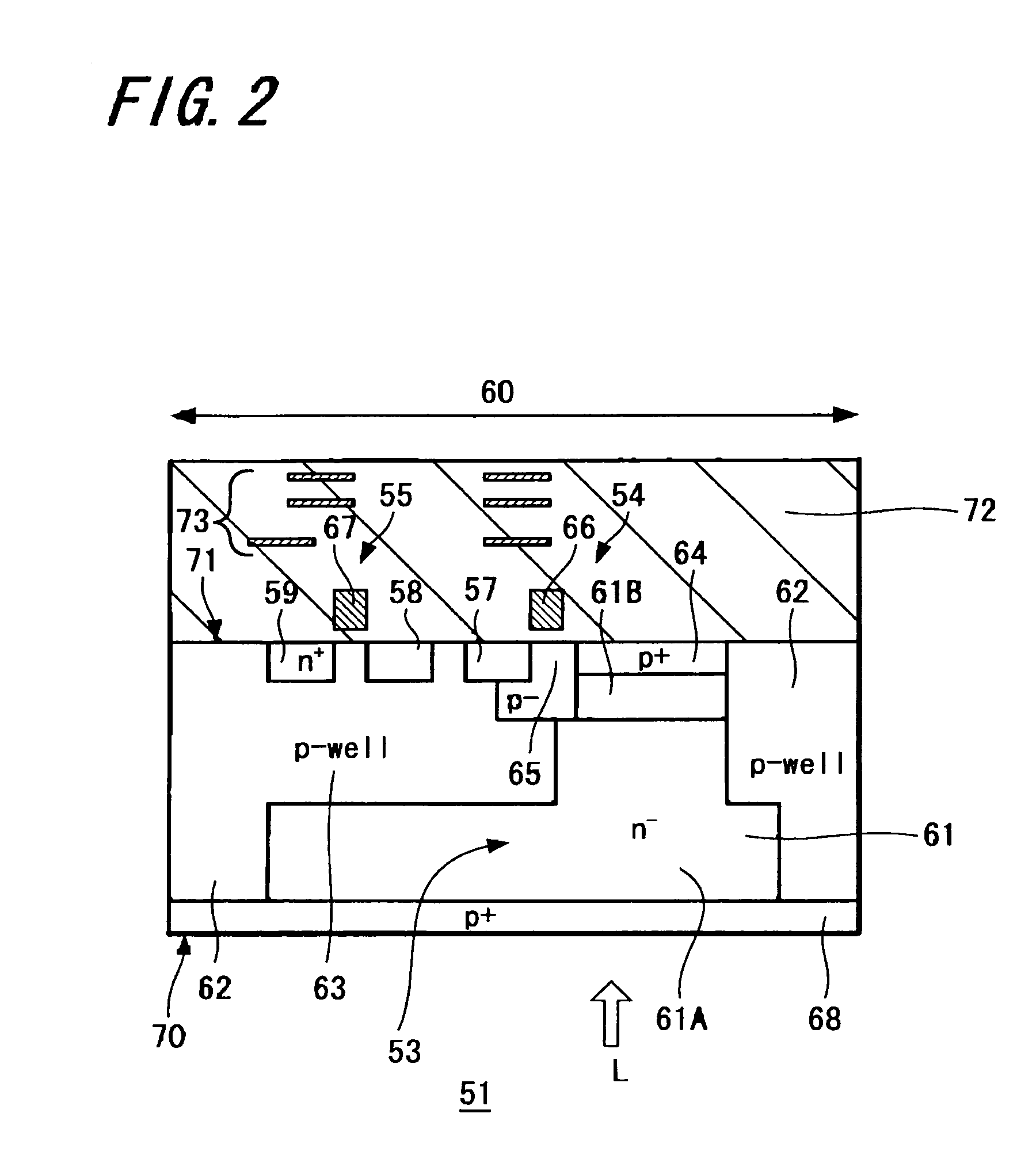
[0040] First, a semiconductor image sensor of a back-illuminated type used for the semiconductor image sensor module according to the present invention will be explained. FIG. 2 is a schematic constitutional diagram showing an embodiment of the semiconductor image sensor of a back-illuminated type to be used for the semiconductor image sensor module according to the present invention, and specifically shows a relevant part in the vicinity of a light-receiving portion that is a photo-sensor.

[0041] As shown in FIG. 2, a back-illuminated type CMOS solid-state imaging device (what is called a semiconductor image sensor) 51 includes: a photo diode 53 to be the light-receiving portion formed in, for example, an n-type silicon substrate 61, a transfer transistor 54 formed on the substrate front surface side of a p-type well region 63 that is contiguous with a p-type pixel separation regi...


PUM


Abstract

A semiconductor image sensor module and a method for manufacturing thereof as well as a camera and a method for manufacturing thereof are provided in which a semiconductor image sensor chip and an image signal processing chip are connected with a minimum parasitic resistance and parasitic capacity and efficient heat dissipation of the image signal processing chip and shielding of light are simultaneously obtained.
A semiconductor image sensor module 1 at least includes a semiconductor image sensor chip 2 having a transistor forming region on a first main surface of a semiconductor substrate and having a photoelectric conversion region with a light incident surface formed on a second main surface on the side opposite to the first main surface and an image signal processing chip 3 for processing image signals formed in the semiconductor image sensor chip 2, wherein a plurality of bump electrodes 15a are formed on a first main surface, a plurality of bump electrodes 15b are formed on the image signal processing chip 3, both the chips 2 and 3 are formed to be laminated through heat dissipating means 4 and the plurality of bump electrodes 15a of the semiconductor image sensor chip 2 and the plurality of bump electrodes 15b on the image signal processing chip 3 are electrically connected.

Description

CROSS REFERENCE TO RELATED APPLICATIONS [0001] The present invention contains subject matter related to Japanese Patent Application JP 2004-311062 filed in Japanese Patent Office on Oct. 26, 2004, the entire contents of which being incorporated herein by reference. BACKGROUND OF THE INVENTION [0002] 1. Field of the Invention [0003] The present invention relates to a semiconductor sensor module in which a semiconductor image sensor chip and a video signal processing chip are mounted and a method for manufacturing the semiconductor sensor module as well as a camera and a method for manufacturing the camera. [0004] 2. Description of the Related Art [0005] In an imaging device such as a digital still camera or digital video camera, a semiconductor image sensor chip such as a CCD image sensor and CMOS image sensor is used. A plurality of components such as image signal processing chips for processing image signals output from an image pickup element of the imaging device and image pickup...

Claims


Application Information

Patent Timeline
IPC IPC(8): H01L27/00H01L31/00H01L27/14H04N5/225H04N5/335H04N5/357H04N5/369H04N5/374H04N101/00
CPCH01L27/14618H01L31/0203H04N5/2257H01L27/14634H01L2924/0002H04N23/57H01L2924/00H01L27/146H04N23/00H01L27/14632H01L27/1464H01L31/024
Inventor YOSHIHARA, IKUOYAMANAKA, MASAMITSU
Owner SONY CORP
Why Eureka
Try Eureka