Metal oxide semiconductor (MOS) transistors having a recessed gate electrode and methods of fabricating the same

a technology of metal oxide semiconductor and gate electrode, which is applied in the direction of transistors, semiconductor devices, electrical equipment, etc., can solve the problems of difficult to effectively control the on/off operation the inability to operate normally of the mos transistor, and the inability to improve the swing or off current characteristi

Active Publication Date: 2006-05-04
SAMSUNG ELECTRONICS CO LTD
View PDF7 Cites 85 Cited by
  • Summary
  • Abstract
  • Description
  • Claims
  • Application Information

AI Technical Summary

Benefits of technology

[0021] In still further embodiments, the buffer layer pat

Problems solved by technology

As a result, a MOS transistor with a typical horizontal channel may not operate normally due to a short channel effect (SCE) and a drain-induced barrier lowering (DIBL) effect, which may be caused by a short channel length between a source and a drain.
Also, owing to increases in off current and swing, it may

Method used


Image

  • Metal oxide semiconductor (MOS) transistors having a recessed gate electrode and methods of fabricating the same
  • Metal oxide semiconductor (MOS) transistors having a recessed gate electrode and methods of fabricating the same
  • Metal oxide semiconductor (MOS) transistors having a recessed gate electrode and methods of fabricating the same

Examples


Embodiment Construction

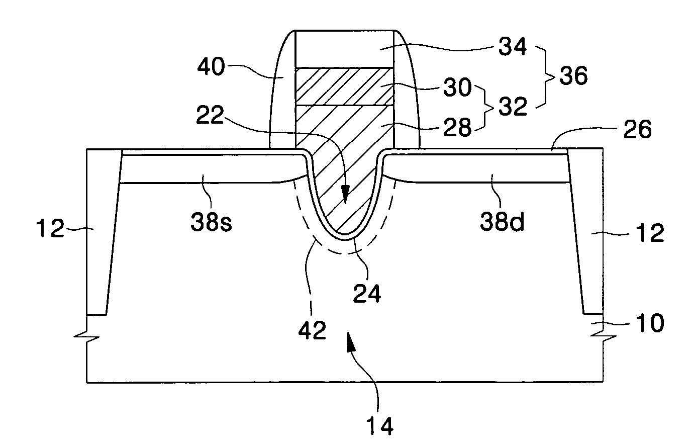
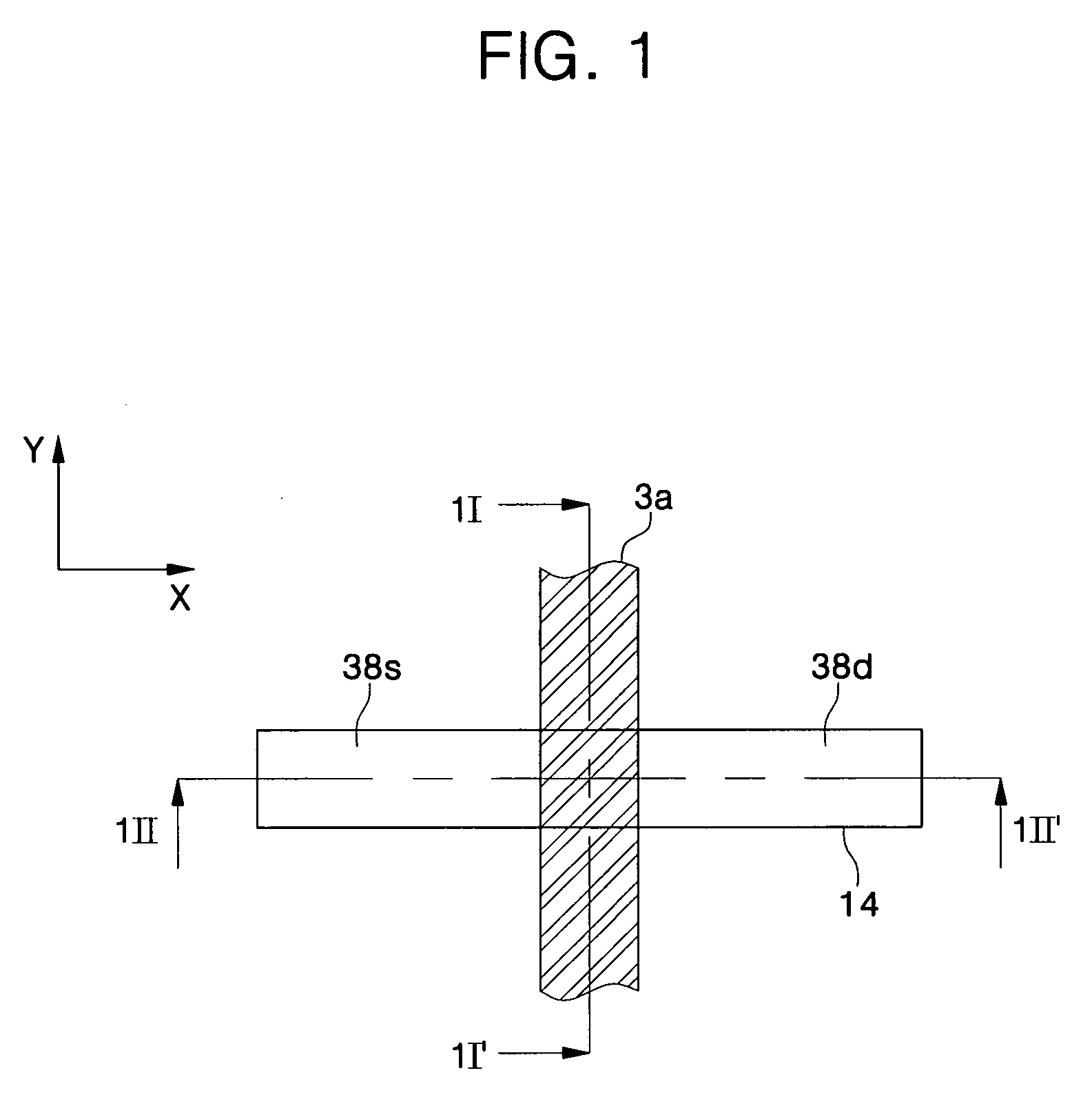
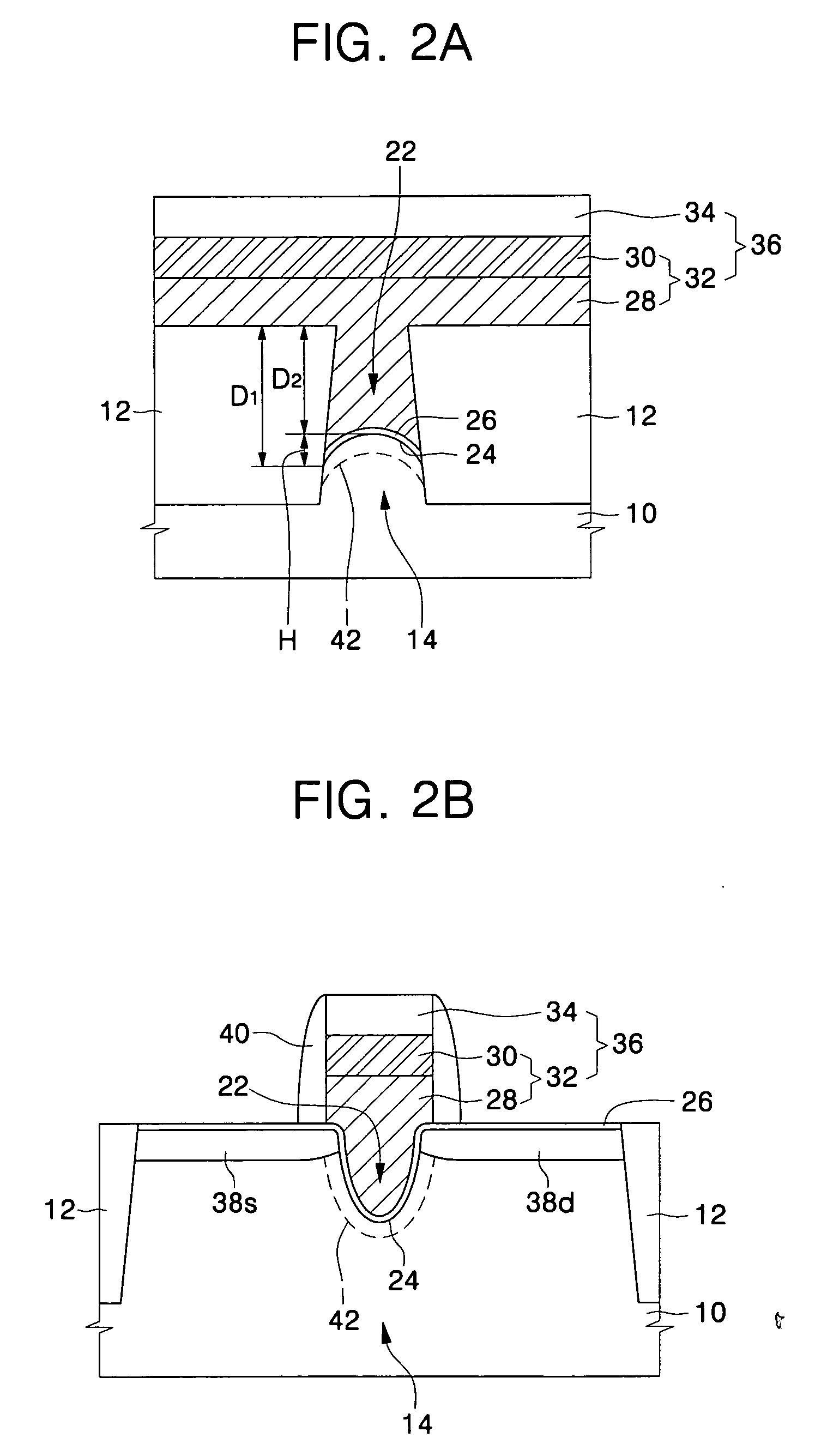
[0029] The invention now will be described more fully hereinafter with reference to the accompanying drawings, in which embodiments of the invention are shown. This invention may, however, be embodied in many different forms and should not be construed as limited to the embodiments set forth herein. Rather, these embodiments are provided so that this disclosure will be thorough and complete, and will fully convey the scope of the invention to those skilled in the art. Like reference numerals refer to like elements throughout the description of the figures.

[0030] It will be understood that when an element is referred to as being “on” another element, it can be directly on the other element or intervening elements may be present. In contrast, when an element is referred to as being “directly on” another element, there are no intervening elements present. As used herein, the term “and / or” includes any and all combinations of one or more of the associated listed items.

[0031] It will b...


PUM


Abstract

A metal oxide semiconductor (MOS) includes an isolation layer disposed in a semiconductor substrate to define an active region. A source region and a drain region are disposed on both sides of the active region such that a first direction is defined from the source region to the drain region. A channel recess is disposed in the active region between the source and drain regions. The channel recess has a convex surface when viewed from a cross-sectional view taken along a second direction orthogonal to the first direction. A gate electrode fills the channel recess and crosses the active region in the second direction. A gate insulating layer is interposed between the gate electrode and the active region.

Description

CROSS-REFERENCE TO RELATED APPLICATION [0001] This application claims the benefit of and priority to Korean Patent Application No. 2004-88512, filed Nov. 2, 2004, the disclosure of which is hereby incorporated herein by reference in its entirety. BACKGROUND OF THE INVENTION [0002] 1. Field of the Invention [0003] The present invention relates generally to semiconductor devices and methods of fabricating the same and, more particularly, to metal oxide semiconductor (MOS) field effect transistors (hereinafter referred to as MOS transistors) and methods of fabricating the same. [0004] 2. Description of Related Art [0005] In general, semiconductor devices use discrete devices, such as MOS transistors as switching devices. With an increase in the degree of integration of semiconductor devices, the MOS transistor is being gradually scaled down. As a result, a MOS transistor with a typical horizontal channel may not operate normally due to a short channel effect (SCE) and a drain-induced b...

Claims


Application Information

Patent Timeline
IPC IPC(8): H01L29/76H01L21/336
CPCH01L29/51H01L29/66621H01L29/7834H01L21/18
Inventor KIM, YOUNG-SUNGCHUNG, TAE-YOUNG
Owner SAMSUNG ELECTRONICS CO LTD
Why Eureka
Try Eureka