High-selectivity etching process

a selective etching and process technology, applied in the direction of basic electric elements, semiconductor/solid-state device manufacturing, electric devices, etc., can solve the problems of loss of pattern fidelity and line-width control, reduced contact area between the via plug and the metal line, and high selective etching selectivity of the etching process, etc., to achieve wider photo latitude, wide etch process window, and high selective etching

Inactive Publication Date: 2006-05-18
MACRONIX INT CO LTD
View PDF8 Cites 16 Cited by
  • Summary
  • Abstract
  • Description
  • Claims
  • Application Information

AI Technical Summary

Benefits of technology

[0008] Due to the high etch selectivity of the etching processes, a wider etch process window can be afforded. Also, this Si-Rich SiON layer allows a wider photo latitude during the photolithography step, because this Si-Rich SiON layer has superior light absorption qualities (acting as an ARC layer).

Problems solved by technology

As the integration of semiconductor devices keeps increasing, the etch selectivity becomes an important issue because poor etch selectivity leads to loss of pattern fidelity and line-width control.
However, the high (large) aspect ratio, due to a small line-width or a deep via hole in the dual damascene structure, or a deep contact opening, can cause difficulties in etching and result in reduced contact area between via plug and the metal line.

Method used


Image

  • High-selectivity etching process
  • High-selectivity etching process
  • High-selectivity etching process

Examples


Embodiment Construction

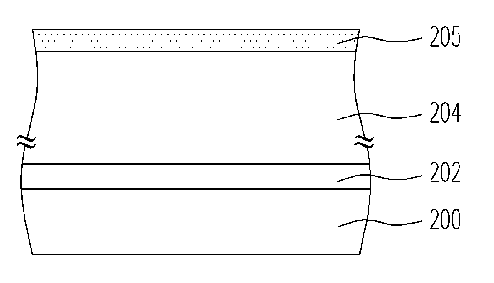
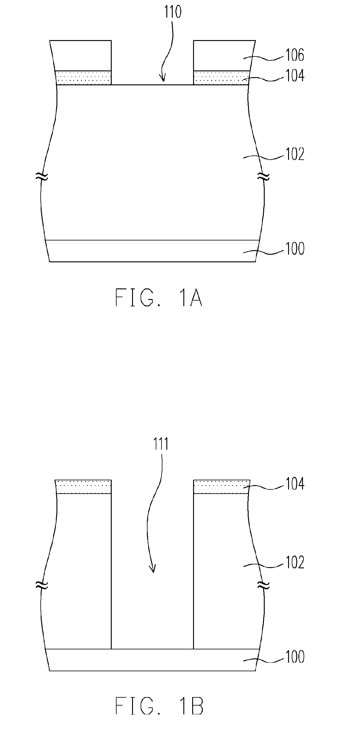
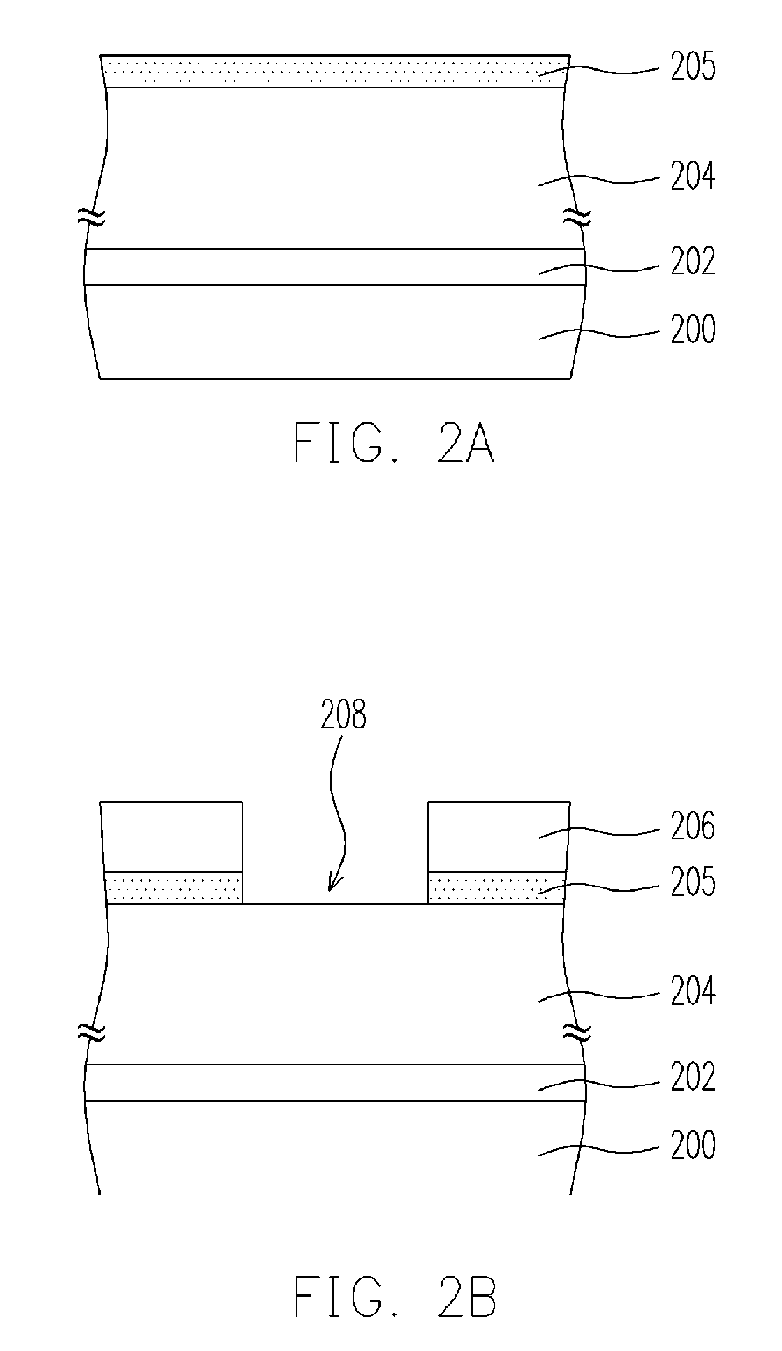
[0015] The present invention provides at least a high-selectivity etching process used for fabricating openings for a contact structure or a dual damascene structure in combination with a Si-rich silicon oxynitride (SiON) barrier layer. The process of this invention is suitable for forming at least an opening for a dual damascene opening or a contact opening, and can be applied in a dual damascene structure, a contact plug, a borderless contact structure or a self aligned contact (SAC) structure.

[0016] The following embodiments provides further descriptions for forming different structures by using at least a highly selective etching process in combination with a Si-rich SiON barrier layer.

[0017] In general, the SiON layer can be formed by plasma enhanced chemical vapor deposition (PECVD), using gaseous mixtures including at least silane (SiH4) and N2O. By changing the deposition parameters and / or the gaseous sources, characteristics and composition of the SiON layer can be varied...


PUM


Abstract

The present invention provides a high-selectivity etching process for fabricating openings for a contact structure or a dual damascene structure in combination with a Si-rich silicon oxynitride (SiON) barrier layer. The process of this invention is suitable for forming at least an opening for a dual damascene opening or a contact opening, and can be applied in a dual damascene structure, a contact plug, a borderless contact structure or a self aligned contact (SAC) structure.

Description

BACKGROUND OF THE INVENTION [0001] 1. Field of Invention [0002] The present invention relates to an etching process for manufacturing semiconductor devices. More particularly, the present invention relates to a high-selectivity etching process for forming openings for a contact structure or a dual damascene structure. [0003] 2. Description of Related Art [0004] During the integrated circuit fabrication processes, lithography and etching processes are frequently repeated for transferring patterns with features for a number of layers of different materials formed sequentially on the wafer. After entering the era of ULSI manufacturing, the etching process becomes more significant for fabricating features with sub-half-micron dimensions. In general, etching can be characterized by the selectivity and degree of anisotropy. Etching can be either physical or chemical, or a combination of both. Wet chemical etching results in isotropic etching, while in dry etching, the wafer is bombarded w...

Claims


Application Information

Patent Timeline
Patent Type & Authority Applications(United States)
IPC IPC(8): H01L21/302
CPCH01L21/31116H01L21/31144H01L21/76802H01L21/7681H01L21/76829H01L21/76897
Inventor HONG, SHIH-PINGHO, CHIAHUA
Owner MACRONIX INT CO LTD
Why Eureka
Try Eureka