Method for removing resin mask layer and method for manufacturing solder bumped substrate

a technology of resin mask and substrate, which is applied in the direction of resist details, photosensitive material processing, electrical apparatus construction details, etc., can solve the problems of resin mask layer residue on the substrate having negative effects on subsequent electronic packaging, affecting the quality of solder bumps on the substrate, and difficult to completely remove resin mask layers. , to achieve the effect of easy removal, short period of time, and easy removal

Active Publication Date: 2006-05-25
HARIMA CHEM INC
View PDF3 Cites 22 Cited by
  • Summary
  • Abstract
  • Description
  • Claims
  • Application Information

AI Technical Summary

Benefits of technology

The present invention provides a method for easily removing a heat-processed resin mask layer without damaging solder resist and solder on a substrate, which improves the reliability of solder connection. The method involves using glycol ethers or aminoalcohols to remove the resin mask layer after heating process. This method allows for a faster and more efficient manufacturing process of circuit substrates.

Problems solved by technology

The technical problem addressed in this patent text is the difficulty of completely removing a resin mask layer that is more resistant to separation after the heating process to form solder bumps, and the possibility of damaging solder resist and solder bumps on a substrate when using a strong alkaline solution as a resist stripping agent. The patent text proposes a method for resist separation that does not require a high temperature heating process.

Method used


Image

  • Method for removing resin mask layer and method for manufacturing solder bumped substrate
  • Method for removing resin mask layer and method for manufacturing solder bumped substrate
  • Method for removing resin mask layer and method for manufacturing solder bumped substrate

Examples


example i

(Substrate)

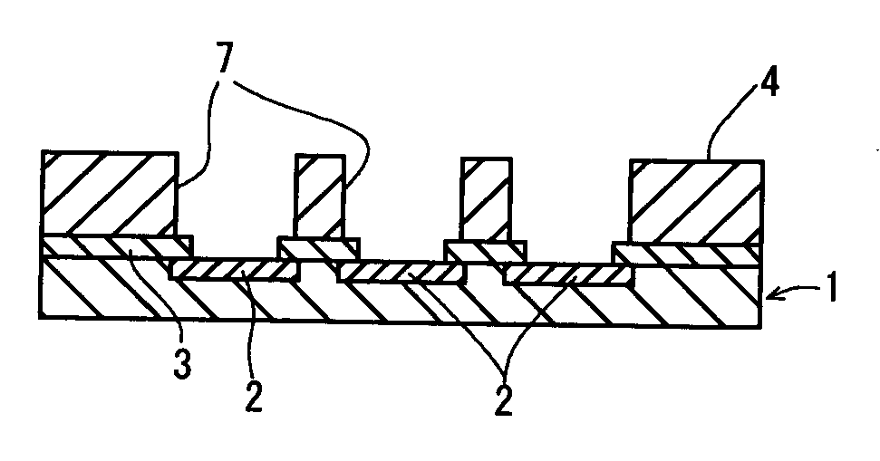
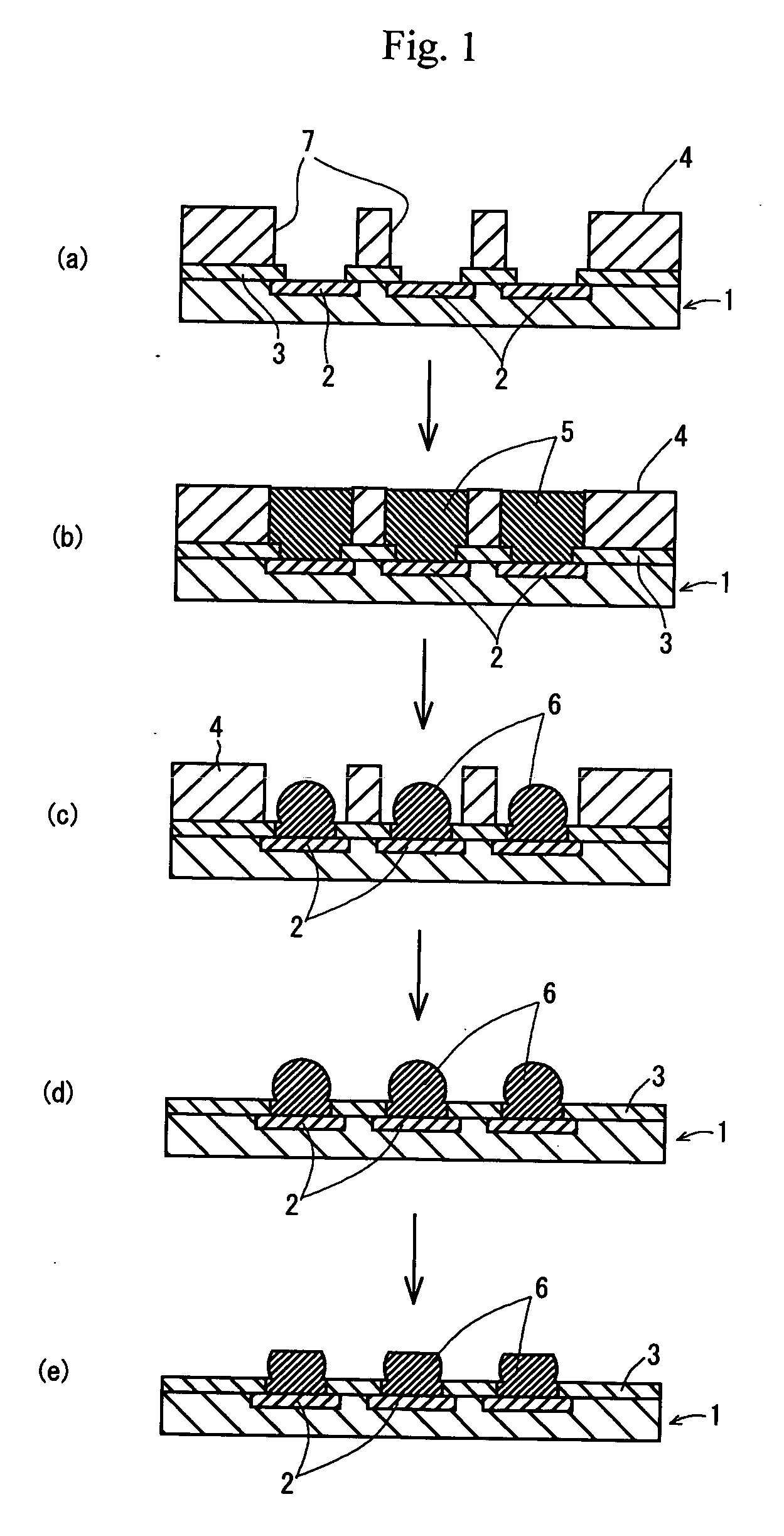
[0061] The substrate used here was covered with a 10 μm thick solder resist film, and had pads (electroless nickel gold plated electrodes) exposed from opening parts (diameter: 80 μm) that were formed in the solder resist film. The pads were formed at 150 μm pitches on the substrate.

(Preparation of Dry Film Resist (a))

[0062] The following ingredients were mixed to prepare a photosensitive resin solution.

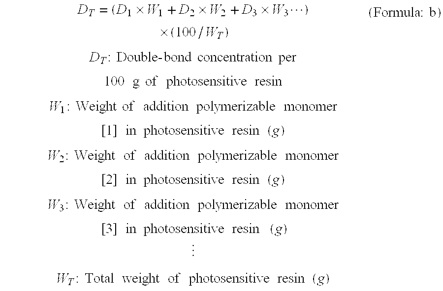
Methyl ethyl ketone solution of a terpolymer of 65% by weight of methyl  65 gmethacrylate, 25% by weight of methacrylic acid and 10% by weight of butylacrylate (concentration of solid content: 34%, weight-average molecular weight:80,000, acid equivalent: 340)Methyl ethyl ketone solution of a terpolymer of 65% by weight of methyl  88 gmethacrylate, 25% by weight of methacrylic acid and 10% by weight of butylacrylate (concentration of solid content: 34%, weight-average molecular weight:120,000, acid equivalent: 340)Triethoxy methylol propane acrylate  10 gDimethacryla...

example 2

[0071] IL of butyl carbitol that was heated to about 60° C. was added in an ultrasonic cleaning equipment. The substrate having a resin mask layer and solder bumps formed in the same manner as in Example 1 was soaked therein and the resin mask layer was removed through ultrasonic cleaning for 3 to 5 minutes.

example 3

[0072] The substrate having a resin mask layer and solder bumps formed in the same manner as in Example 1 was soaked in the remover of 20° C. obtained in Example 1 for 30 minutes to remove the resin mask layer.


PUM

PropertyMeasurementUnit
Temperatureaaaaaaaaaa
Percent by massaaaaaaaaaa

Abstract

Using a dry film resist that is a photosensitive resin, a resin mask layer is formed around electrodes on a substrate. A solder precipitating composition is applied on the substrate, and this solder precipitating composition is heated to precipitate solder on the surface of the electrodes. Subsequently, in removing the resin mask layer, at least one selected from glycol ethers and aminoalcohols is used. Thereby, the resin mask layer is removed after heating process. This makes it possible to easily remove the heat-processed resin mask layer in a short period of time without damaging solder resist and solder bumps on the substrate.

Description


Claims


Application Information

Patent Timeline
Owner HARIMA CHEM INC
Why Eureka
Try Eureka