Pixel interpolation method and image distinction method

a pixel interpolation and image technology, applied in the field of pixel interpolation technique, can solve the problems of image positioned on the boundary between a gray image and a color image degrading in picture quality, and achieve the effects of reducing color aliasing, high-quality sharp image, and improving resolution

Inactive Publication Date: 2006-06-01
MEGACHIPS
View PDF9 Cites 32 Cited by
  • Summary
  • Abstract
  • Description
  • Claims
  • Application Information

AI Technical Summary

Benefits of technology

[0008] An object of the present invention is to provide an image processing method capable of ...

Problems solved by technology

However, a conventional interpolation method causes in some cases degradation in picture quality due to misinterpolation in a gray image containing high-frequency components...

Method used


Image

  • Pixel interpolation method and image distinction method
  • Pixel interpolation method and image distinction method
  • Pixel interpolation method and image distinction method

Examples


first preferred embodiment

1. General Overall Construction of Digital Camera

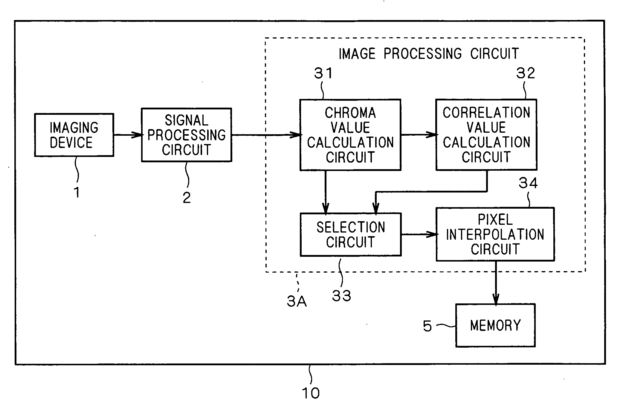
[0037]FIG. 1 is a block diagram illustrating a digital camera 10 according to a first preferred embodiment of the present invention. The digital camera 10 includes an imaging device 1, a signal processing circuit 2, an image processing circuit 3A and a memory 5. The imaging device 1 is a single-chip CCD having a color filter array of RGB Bayer pattern, and outputs a pixel signal of one of RGB color components per pixel. More specifically, assuming that a G signal and an R signal are output alternately like GRGR in an odd-numbered horizontal line, a B signal and a G signal are output alternately like BGBG in an even-numbered horizontal line. A CMOS sensor may be used as the imaging device 1.

[0038] A pixel signal output from the imaging device 1 is input to the signal processing circuit 2. The signal processing circuit 2 executes signal processing such as white balance and black level correction on the pixel signal. The pixel signal ...

second preferred embodiment

[0107]FIG. 18 is a block diagram illustrating a digital camera 10 according to a second preferred embodiment of the present invention. The present embodiment differs from the first preferred embodiment in that the image processing circuit 3A is replaced by an image processing circuit 3B.

[0108] The image processing circuit 3B includes the chroma value calculation circuit 31 similarly to the image processing circuit 3A, but without the selection circuit 33, and includes correlation value calculation circuits 321 and 322 instead of the correlation value calculation circuit 32 and pixel interpolation circuits 341 and 342 instead of the pixel interpolation circuit 34, and further includes a synthesis circuit 35.

[0109] The correlation value calculation circuits 321 and 322 according to the present embodiment calculate a correlation value for color image and a correlation value for gray image, respectively, to determine a correlated direction on the basis of the correlation values. Corre...

third preferred embodiment

[0118]FIG. 21 is a block diagram illustrating a digital camera 10 according to a third preferred embodiment of the present invention. The present embodiment differs from the first preferred embodiment in that the image processing circuit 3A is replaced by an image processing circuit 3C.

[0119] The image processing circuit 3C includes the chroma value calculation circuit 31, pixel interpolation circuits 341, 342 and synthesis circuit 35 similarly to the image processing circuit 3B, and includes a correlation value calculation circuit 323 instead of the correlation value calculation circuits 321 and 322.

[0120] The operation of the chroma value calculation circuit 31 has been described in the first preferred embodiment, and operations of the pixel interpolation circuits 341, 342 and synthesis circuit 35 have been described in the second preferred embodiment. Accordingly, repeated explanation will be omitted in this preferred embodiment.

[0121] The correlation value calculation circuit...


PUM


Abstract

An image processing circuit inputs pixels arranged in RGB Bayer pattern. A chroma value calculation circuit calculates a chroma coefficient for evaluating chroma of a peripheral region of a target pixel. A correlation value calculation circuit calculates a correlation value for gray image and a correlation value for color image. When the chroma coefficient is higher than a first threshold value, a correlation judging method for color image and a pixel interpolation method for color image are selected. When the chroma coefficient is not higher than the first threshold value and higher than a second threshold value, a correlation judging method for gray image and the pixel interpolation method for color image are selected. When the chroma coefficient is not higher than the second threshold value, the correlation judging method for gray image and a pixel interpolation method for gray image are selected. Interpolation is executed in a pixel interpolation circuit.

Description

BACKGROUND OF THE INVENTION [0001] 1. Field of the Invention [0002] The present invention relates to a pixel interpolation technique adopted in an image processing circuit provided for a digital camera or the like. [0003] 2. Description of the Background Art [0004] An imaging device such as CCD or CMOS used in a digital camera or the like photoelectrically transfers light received through a color filter to output a pixel signal. Such color filter includes an RGB color filter, a YMCK color filter and the like. A single-chip imaging device outputs a single-color pixel signal per pixel. For instance, when employing the RGB color filter, a pixel signal having one of R (red), G (green) and B (blue) color components is output per pixel. [0005] Therefore, a pixel signal output from a single-chip color imaging device needs to be interpolated with pixel signals of other color components. Various algorithms are used in such interpolation. An exemplary method is to calculate a correlation in t...

Claims


Application Information

Patent Timeline
IPC IPC(8): G03F3/08
CPCG06T3/4015H04N2101/00
Inventor HASEGAWA, HIROMU
Owner MEGACHIPS
Why Eureka
Try Eureka