Optical communication system

a communication system and optical technology, applied in the field of optical communication systems, can solve the problems of propagation errors occurring in high-speed transmissions that cannot be prevented, and achieve the effect of reducing communication errors in high-speed transmissions

Inactive Publication Date: 2006-06-01
FUJIFILM BUSINESS INNOVATION CORP +1
View PDF8 Cites 3 Cited by
  • Summary
  • Abstract
  • Description
  • Claims
  • Application Information

AI Technical Summary

Benefits of technology

[0021] According to the present invention as described above, it is possib...

Problems solved by technology

Thus, with optical coupling structures for which coupling of optical elements with light propagation mediums such that light energies are at maximum ...

Method used


Image

  • Optical communication system
  • Optical communication system
  • Optical communication system

Examples


first embodiment

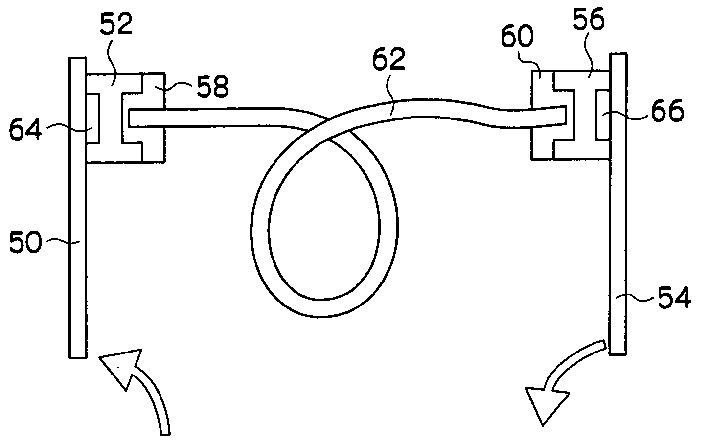
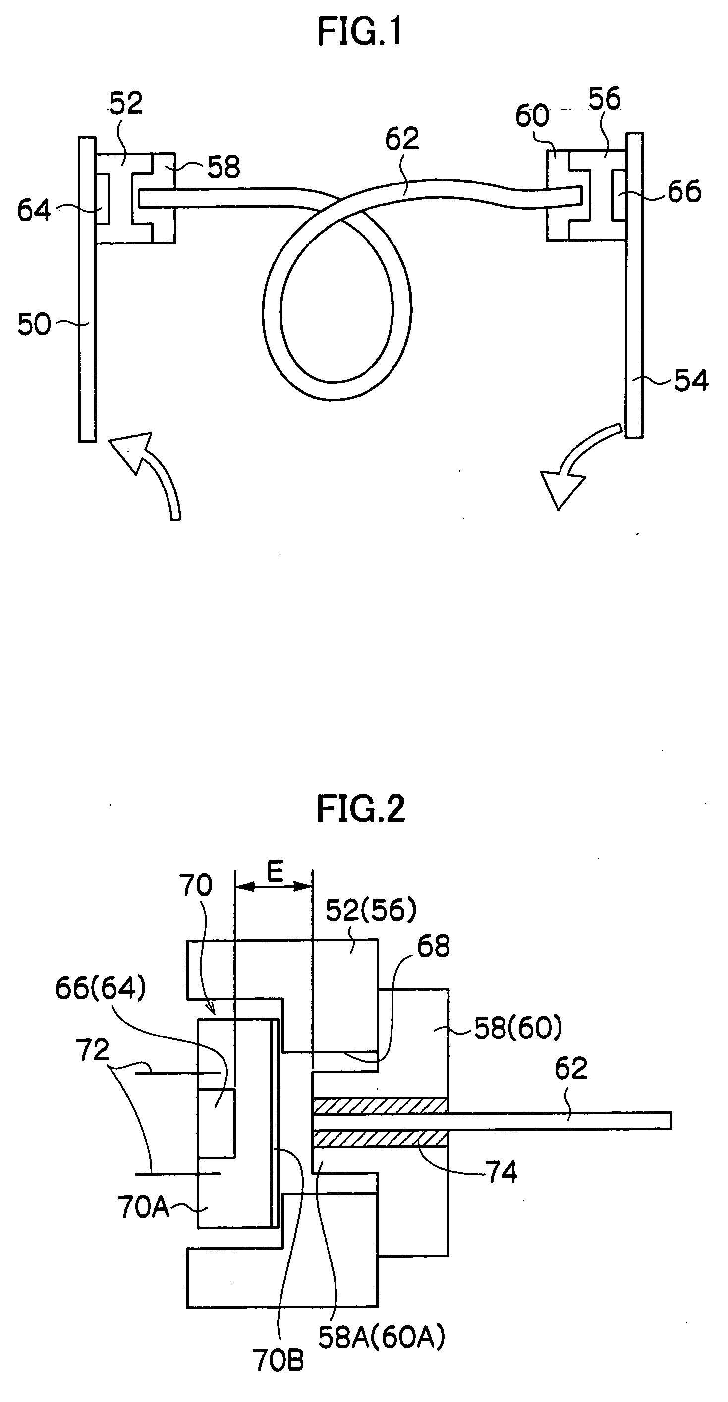
[0041] A first embodiment of the present invention, which relates to an optical coupling structure between an optical element and an optical transmission medium of the present invention and to an optical linking system (corresponding to an optical communication system) which employs this optical coupling structure, will be described in accordance with FIGS. 1 to 6 and FIGS. 12 to 16.

[0042] As shown in FIG. 1, an optical linking system relating to this first embodiment is provided with a transmitter 50 (corresponding to a first signal communication apparatus), a receptacle 52, a receiver 54 (corresponding to a second signal communication apparatus), a receptacle 56, and an optical fiber cable (a multimode optical fiber) 62 (corresponding to an optical transmission medium / an optical signal propagation medium). The transmitter 50 is equipped with a circuit which converts inputted electronic signals to optical signals. The receptacle 52 is disposed at the transmitter 50. The receiver 5...

second embodiment

[0068] Next, a second embodiment relating to the present invention will be described with reference to FIGS. 7 to 12.

[0069] In the present embodiment, a structure which is provided with a collector lens 80 is employed as the transmitter 50 side receptacle 52 (and / or the receiver 54 side receptacle 56) for structuring the optical coupling component.

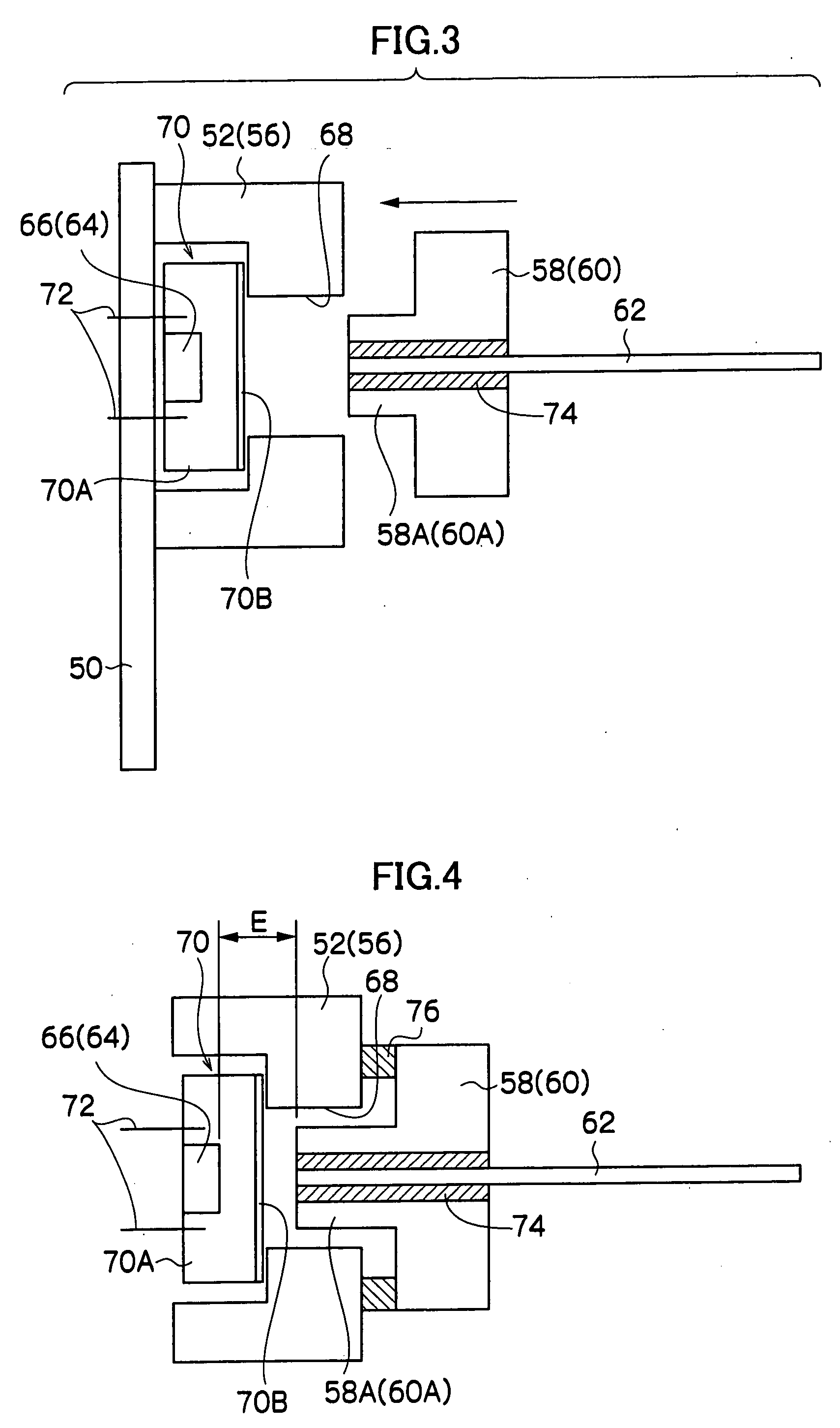
[0070] At the transmitter 50 side receptacle 52 (or the receiver 54 side receptacle 56) which employs this collector lens, as shown by the examples in FIGS. 7 and 8, a light guide aperture 84 is formed through a floor portion of the coupling insertion hole 68, which is formed in a housing 82 of the receptacle 52 (or 56). The collector lens 80 is disposed in the housing 82 at the optical element package 70 side relative to the light guide aperture 84.

[0071] At this housing 82, the optical element package 70 is disposed on a path of light which is focused by the collector lens 80. The optical element package 70 has a structure in which th...


PUM


Abstract

The present invention provides a method for reducing propagation errors in an optical communication system which includes an optical element and an optical transmission medium. In the present invention, a relative position of the optical element and an end face of the optical transmission medium, at which light emitted from the optical element is incident, is set to a (relative) position which is different from a relative position of the optical element and the end face of the optical transmission medium with which energy of light that is propagated is maximized. Then, light emitted from the optical element is propagated in multimode by the optical transmission medium.

Description

CROSS-REFERENCE TO RELATED APPLICATION [0001] This application claims priority under 35 USC 119 from Japanese Patent Application No. 2004-348853, the disclosure of which is incorporated by reference herein. BACKGROUND OF THE INVENTION [0002] 1. Field of the Invention [0003] The present invention relates to an optical communication system. More particularly, the present invention relates to an optical communication system, a method for reducing errors in an optical communication system, a butt-optical-coupling structure for an optical element and an optical transmission medium, and an optical coupling structure for an optical element and an optical transmission medium. [0004] 2. Description of the Related Art [0005] In recent years, optical linking systems have been employed in the field of optical communications, in which digital apparatuses such as electronic equipment and the like are connected with one another and long-distance propagation of high-speed signals that is not possib...

Claims


Application Information

Patent Timeline
IPC IPC(8): H04B10/12G02B6/42
CPCG02B6/4202G02B6/4206G02B6/4292H04B10/2581
Inventor YAMADA, HIDENORINIITSU, TAKEHIROKYOZUKA, SHINYASUZUKI, KAZUHIROBABA, TOMOOZEKI, SHINOBUYOSHIMURA, KOUICHIROSUGIMOTO, ATSUNOBU
Owner FUJIFILM BUSINESS INNOVATION CORP
Why Eureka
Try Eureka