Semiconductor device and method for manufacturing the same

a semiconductor and capacitor technology, applied in the field of metalinsulators, can solve the problems of destabilizing the voltage applied to the electrode, the capacitance value of the capacitor is not uniformly maintained, and the limits of polycrystalline silicon are unable to reduce the inherent electrical resistance of the constituent electrode, etc., to achieve the effect of improving the capacitance of the mim capacitor

Inactive Publication Date: 2006-06-08
SAMSUNG ELECTRONICS CO LTD
View PDF9 Cites 34 Cited by
  • Summary
  • Abstract
  • Description
  • Claims
  • Application Information

AI Technical Summary

Problems solved by technology

However, this use of the mono-crystalline silicon or a polycrystalline silicon limits attempts to reduce the inherent electrical resistance of the constituent electrode.
As a result, if a bias voltage is applied to the mono-crystalline silicon or polycrystalline silicon electrode, a depletion region may form, thereby destabilizing the voltage applied to the electrode.
When this happens, the capacitance value of the capacitor is not uniformly maintained.
As lateral layout space in semiconductor devices comes at an increasing premium, this conventional arrangement suffers from real limits in a designer's ability to increase the overall capacitance of the MIM capacitor.
Indeed, as emerging design rules mandate smaller MIM capacitors, the conventional design fails to provide sufficient capacitance.

Method used


Image

  • Semiconductor device and method for manufacturing the same
  • Semiconductor device and method for manufacturing the same
  • Semiconductor device and method for manufacturing the same

Examples


Embodiment Construction

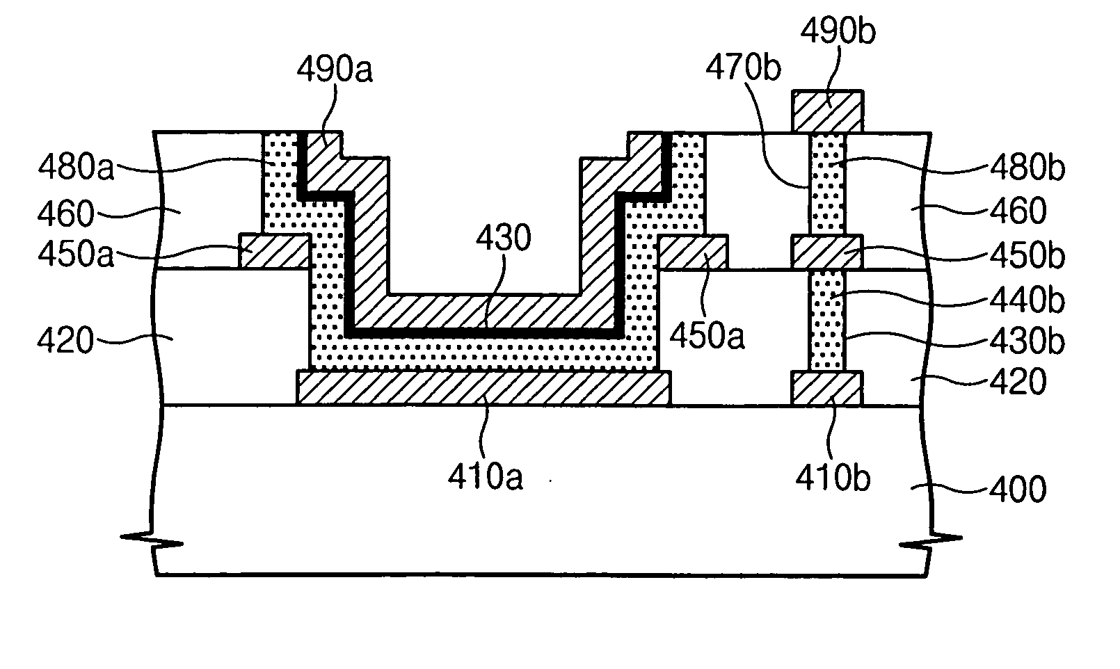
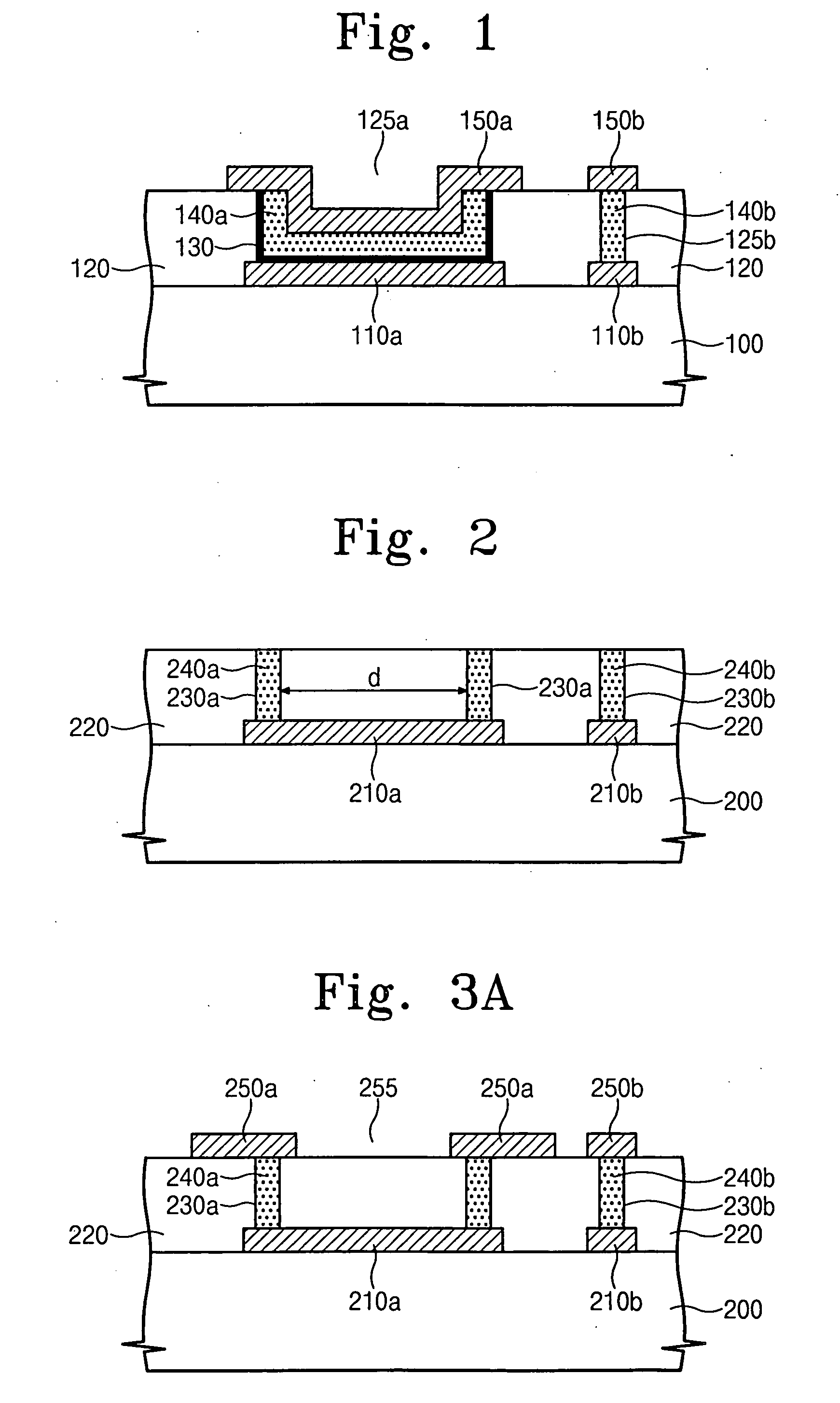
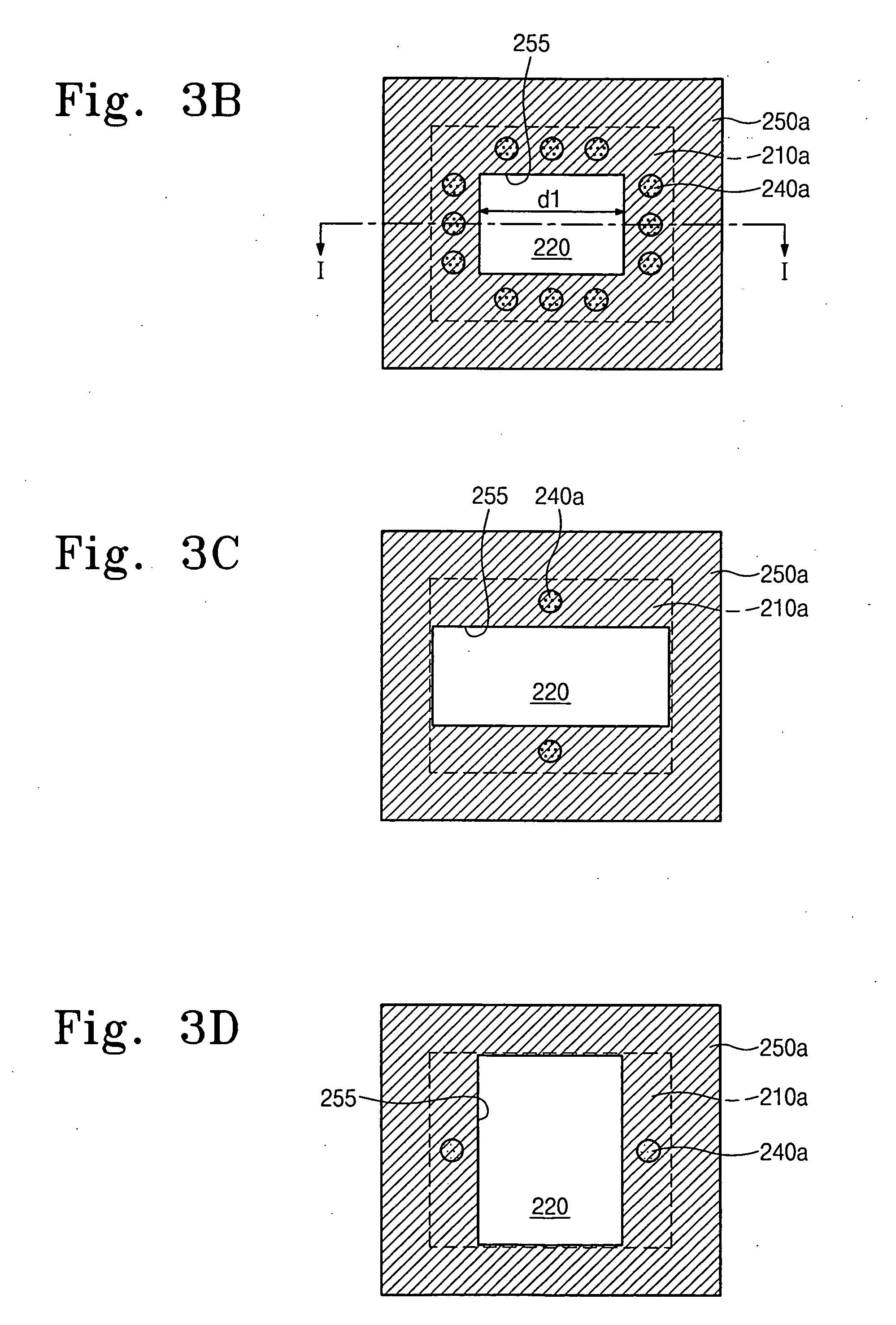
[0022] The invention will now be described in some additional detail with reference to the accompanying drawings and in relation to several exemplary embodiments. The invention may, however, be embodied in many different forms beyond the exemplary embodiments, and should not be constructed as being limited to only the illustrated examples. Throughout the description that follows, the term “on” is used to describe a relationship between layers and / or elements in the exemplary embodiments. This term should be construed as covering layers and / or elements directly on one another, as well as layers and / or elements being “on” one another, but possibly having one or more intervening layers and / or elements in between.

[0023] FIGS. 2 to 7 are related cross-sectional views illustrating a manufacturing method and a resulting structure for a MIM capacitor in accordance with one embodiment of the invention.

[0024] Referring to FIG. 2, a first metal pattern 210a and a first metal interconnection ...


PUM

PropertyMeasurementUnit
dielectric constantaaaaaaaaaa
conductiveaaaaaaaaaa

Abstract

Disclosed is a metal-insulator-metal (MIM) capacitor structure formed by a metal interconnection process of trench-exposed metal layers formed on stacked interlayer insulating layers. The MIM capacitor uses a conductive layer conformally formed on the metal interconnection and / or trench regions to enlarge constituent electrode surface areas.

Description

BACKGROUND OF THE INVENTION [0001] Embodiments of the present invention relate generally to a metal-insulator-metal (referred to as “MIM” hereinafter) capacitor structure having high capacitance, and an integrated circuit chip including same. [0002] This application claims the benefit of Korean Patent Application 2004-101183 filed on Dec. 3, 2004, the contents of which are hereby incorporated by reference. [0003] Capacitors may be classified accordingly to their junction structure, for example, as metal-oxide-silicon (MOS), p-n junction, polysilicon-insulator-polysilicon (PIP), metal-insulator-metal (MIM), etc. All the above-mentioned examples, except MIM capacitors, comprise at least one electrode material formed from a mono-crystalline silicon or polycrystalline silicon material. However, this use of the mono-crystalline silicon or a polycrystalline silicon limits attempts to reduce the inherent electrical resistance of the constituent electrode. As a result, if a bias voltage is ...

Claims


Application Information

Patent Timeline
Patent Type & Authority Applications(United States)
IPC IPC(8): H01L21/20H01L29/00
CPCH01L23/5223H01L28/91H01L2924/0002H01L2924/00H01L27/04
Inventor PARK, DUK-SEO
Owner SAMSUNG ELECTRONICS CO LTD
Why Eureka
Try Eureka