Integrated circuit devices including a MIM capacitor

a technology of integrated circuit devices and capacitors, which is applied in the direction of capacitors, semiconductor devices, semiconductor/solid-state device details, etc., can solve the problems of insufficient distance between the interconnection layer, performance of mim capacitors, and the difficulty of obtaining the desired capacitance in a conventional metal-insulator-semiconductor (mis) capacitor

Active Publication Date: 2005-09-06
SAMSUNG ELECTRONICS CO LTD
View PDF3 Cites 42 Cited by
  • Summary
  • Abstract
  • Description
  • Claims
  • Application Information

AI Technical Summary

Benefits of technology

[0021]In further embodiments of the present invention, the first IMD includes a trench that has a diameter greater than the diameter of the first via hole and a depth that is smaller than the depth of the first via hole. The second IMD may also include a trench that has a diameter greater than the diameter of the second via hole and a depth that is smaller than the depth of the second via hole. The landing pad type independent interconnection layer may be formed to the same height as the first IMD. The landing pad type independent interconnection layer may include a plurality of interconnections that are separated from each other. The upper portion of the landing pad type independent interconnection layer may be wider than the lower portion thereof. Alternatively, the interconnection layer, which is connected to the upper electrode of the MIM capacitor, may be formed to the same height as the second IMD.

Problems solved by technology

As the integration density of integrated circuit devices has increased, it has become more difficult to obtain a desired capacitance in a conventional Metal-Insulator-Semiconductor (MIS) capacitor, for example, due to a low k-dielectric layer formed between a dielectric layer and a silicon layer.
One limitation on the performance of the MIM capacitor illustrated in FIG. 1 is the insufficient distance between the interconnection layer 27 and the lower electrode 21.
As this distance is reduced, an undesirable level of parasitic capacitance may develop, which parasitic capacitance may adversely affect the characteristics of the MIM capacitor.
Problems become more severe when the thickness of the insulating layers is reduced, because parasitic capacitance of the device is generally inversely proportional to the thickness of the insulating layer.
In addition, the variability of the parasitic capacitance based on process variables such as the thickness of an insulating layer may increase the difficulty of forming MIM capacitors with stable characteristics.

Method used


Image

  • Integrated circuit devices including a MIM capacitor
  • Integrated circuit devices including a MIM capacitor
  • Integrated circuit devices including a MIM capacitor

Examples


Embodiment Construction

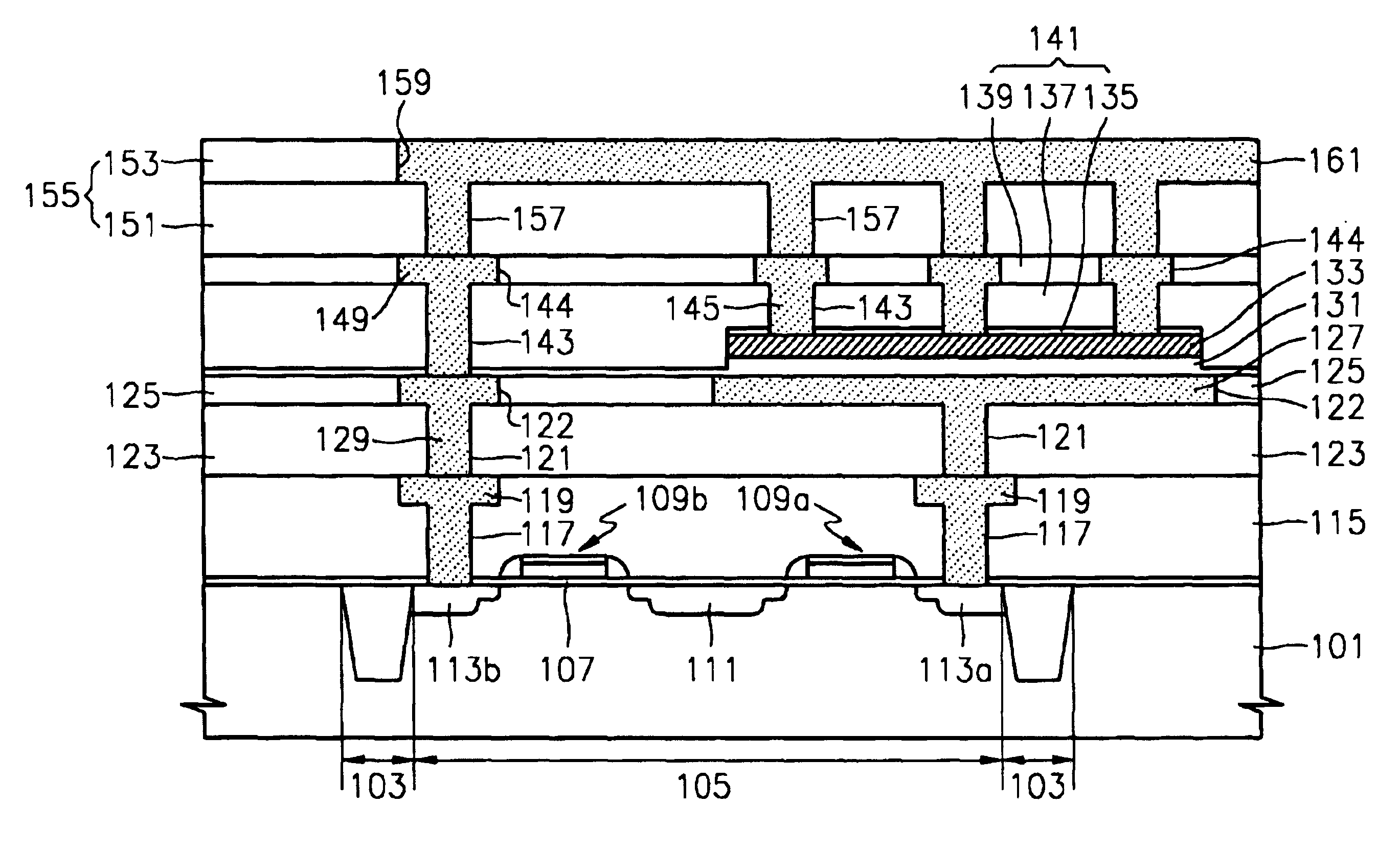
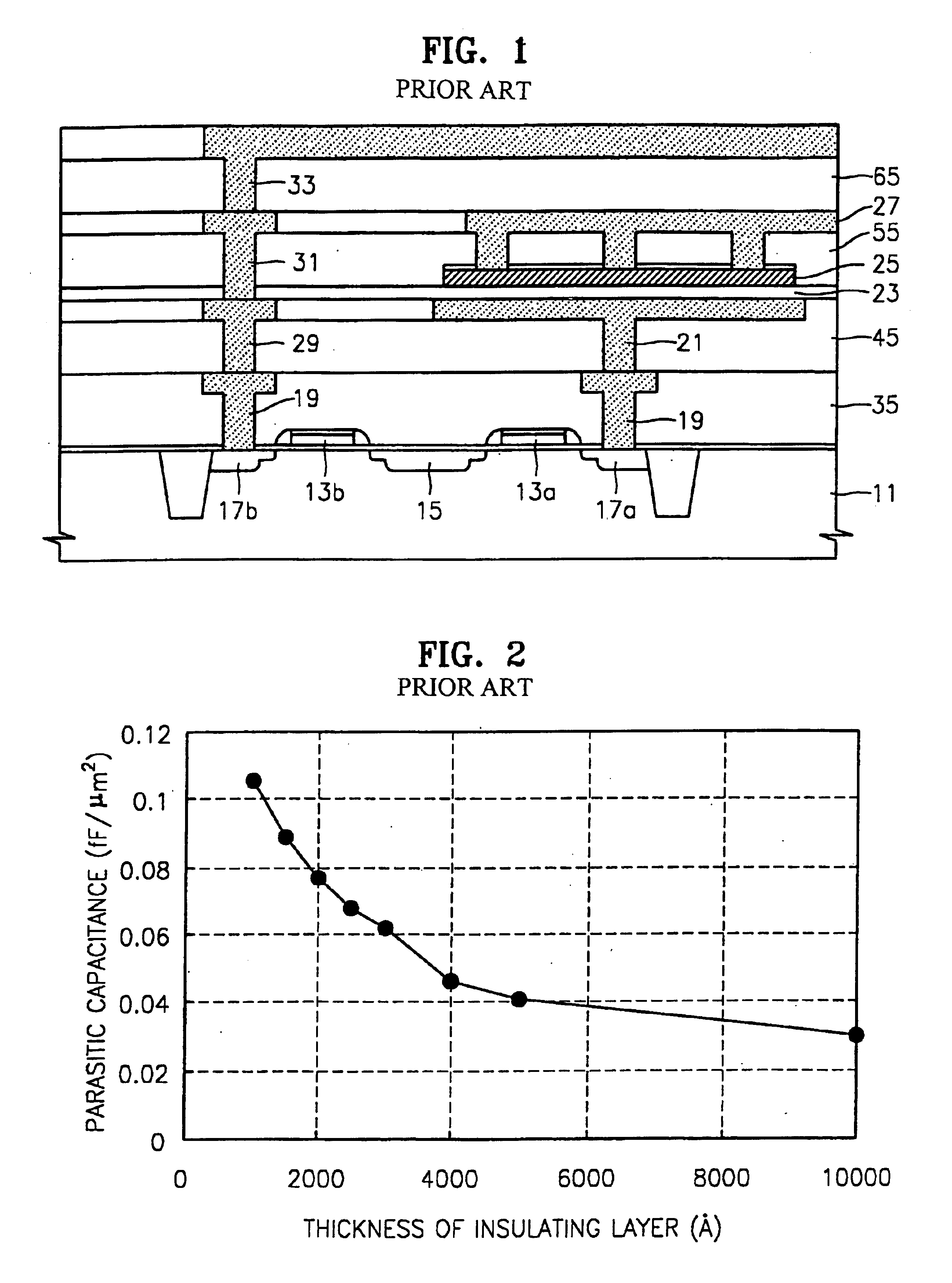
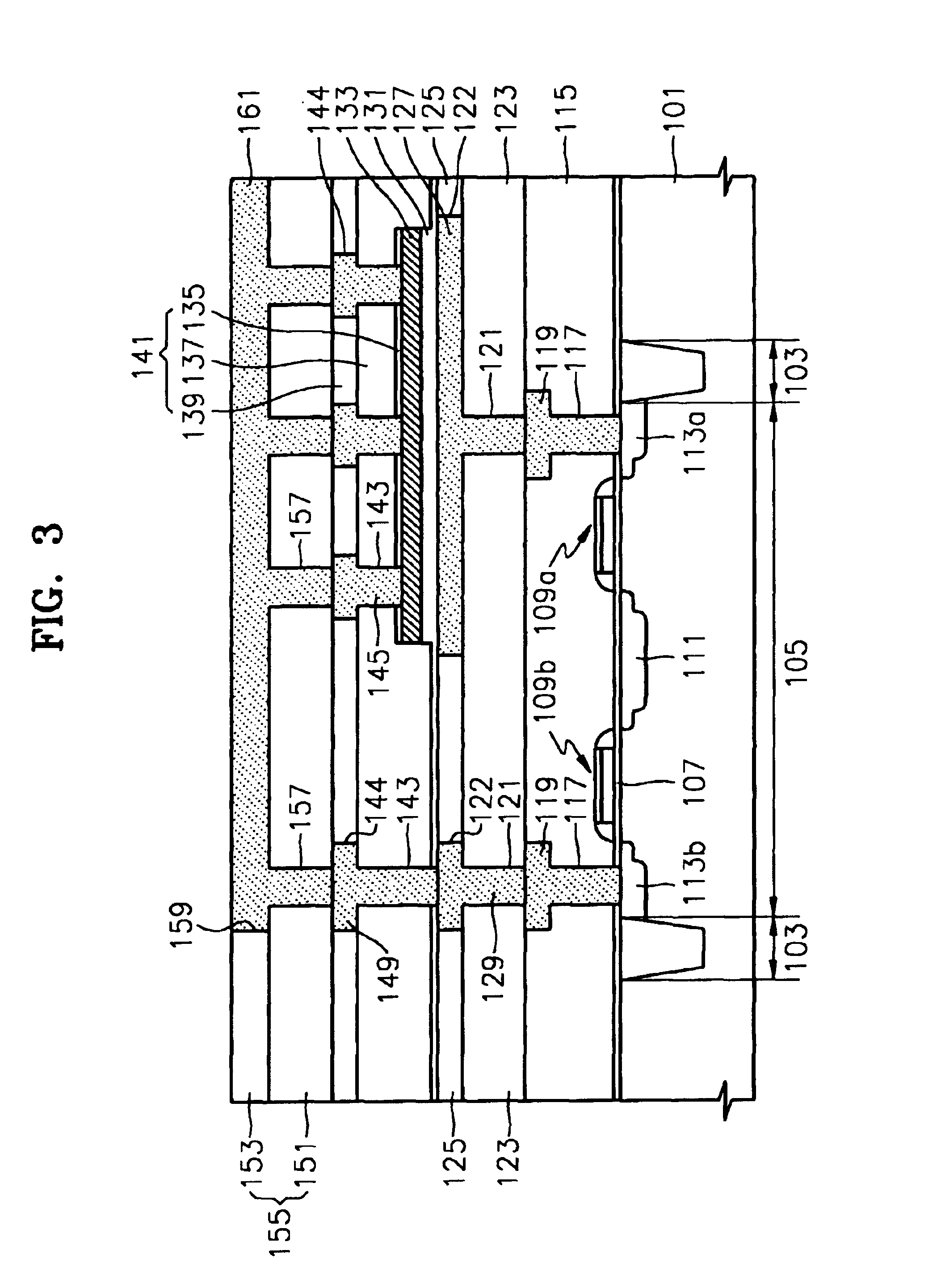
[0030]The present invention now will be described more fully hereinafter with reference to the accompanying drawings, in which typical embodiments of the invention are shown. This invention may, however, be embodied in many different forms and should not be construed as limited to the embodiments set forth herein. Rather, these embodiments are provided so that this disclosure will be thorough and complete, and will fully convey the scope of the invention to those skilled in the art. In the drawings, the relative sizes and shapes of regions may be exaggerated for clarity. It will be understood that when an element such as a layer, region or substrate is referred to as being “on” another element, it can be directly on the other element or intervening elements may also be present. In contrast, when an element is referred to as being “directly on” another element, there are no intervening elements present. Moreover, each embodiment described and illustrated herein includes its complemen...


PUM


Abstract

Integrated circuit devices include an integrated circuit substrate and a conductive lower electrode layer of a Metal-Insulator-Metal (MIM) capacitor on the integrated circuit substrate. A dielectric layer is on the lower electrode layer and a conductive upper electrode layer of the MIM capacitor is on the dielectric layer. A first intermetal dielectric layer is on the upper electrode layer. The first intermetal dielectric layer includes at least one via hole extending to the upper electrode layer. A first conductive interconnection layer is on the at least one via hole of the first intermetal dielectric layer. A second intermetal dielectric layer is on the first intermetal dielectric layer. The second intermetal dielectric layer includes at least one via hole extending to the first conductive interconnection layer and at least partially exposing the at least one via hole of the first intermetal dielectric layer. A second conductive interconnection layer is provided in the at least one via hole of the second intermetal dielectric layer that electrically contacts the first conductive interconnection layer.

Description

RELATED APPLICATION[0001]This application claims priority from Korean Application No. 2002-78905, filed Dec. 11, 2002, the disclosure of which is hereby incorporated herein by reference.BACKGROUND OF THE INVENTION[0002]The present invention relates to integrated circuit devices and, more particularly, integrated circuit devices including capacitors and methods for manufacturing such integrated circuit devices.[0003]As the integration density of integrated circuit devices has increased, it has become more difficult to obtain a desired capacitance in a conventional Metal-Insulator-Semiconductor (MIS) capacitor, for example, due to a low k-dielectric layer formed between a dielectric layer and a silicon layer. An alternative to an MIS capacitor is a metal-insulator-metal (MIM) capacitor.[0004]FIG. 1 is a cross-sectional diagram illustrating an integrated circuit (semiconductor) device including a conventional MIM capacitor coupled to a transistor. As shown in FIG. 1 a first transistor ...

Claims


Application Information

Patent Timeline
Patent Type & Authority Patents(United States)
IPC IPC(8): H01L21/70H01L23/52H01L21/822H01L27/108H01L21/768H01L27/08H01L27/00H01L27/04H01L21/02H01L21/3205H01L23/522H01L27/06
CPCH01L21/76801H01L21/76838H01L23/5223H01L27/0688H01L28/40H01L28/60H01L21/76895H01L27/10852H01L2924/0002H01L2924/00H10B12/033H10B12/00
Inventor OH, BYUNG-JUNLEE, KYUNG-TAEJUNG, MU-KYENG
Owner SAMSUNG ELECTRONICS CO LTD
Why Eureka
Try Eureka