Insulator, capacitor with the same and fabrication method thereof, and method for fabricating semionductor device

Active Publication Date: 2010-04-15
KEY FOUNDRY CO LTD
View PDF5 Cites 36 Cited by
  • Summary
  • Abstract
  • Description
  • Claims
  • Application Information

AI Technical Summary

Benefits of technology

[0006]An embodiment of the present invention is directed to an insulator that can

Problems solved by technology

These methods, however, may degrade

Method used


Image

  • Insulator, capacitor with the same and fabrication method thereof, and method for fabricating semionductor device
  • Insulator, capacitor with the same and fabrication method thereof, and method for fabricating semionductor device
  • Insulator, capacitor with the same and fabrication method thereof, and method for fabricating semionductor device

Examples


embodiments

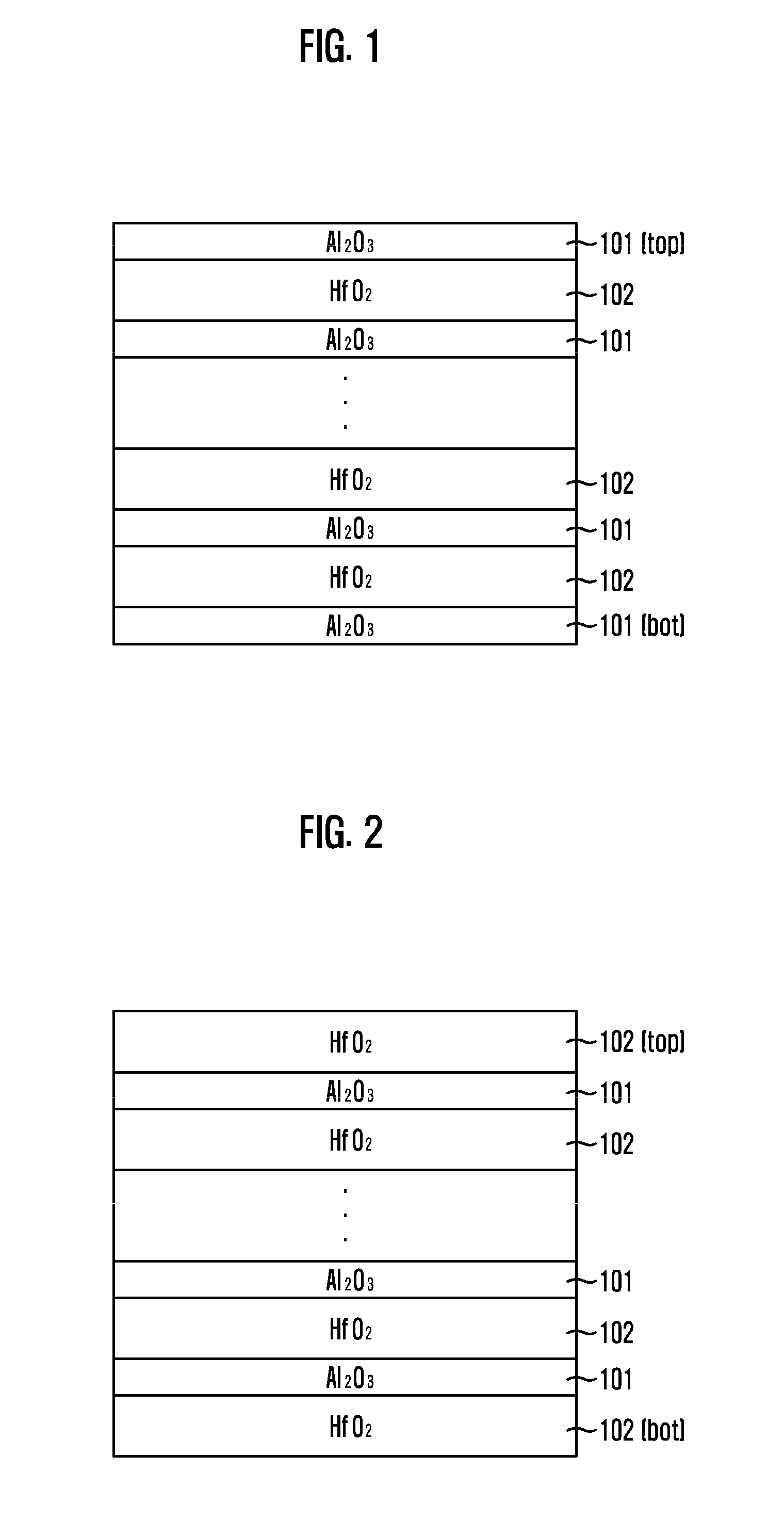
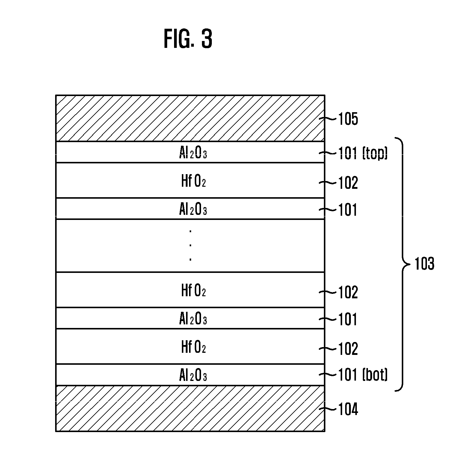
[0029]FIGS. 1 and 2 are cross-sectional views of insulators in accordance with exemplary embodiments of the present invention.

[0030]Referring to FIGS. 1 and 2, an insulator in accordance with an exemplary embodiment of the present invention has a laminate structure where an aluminum oxide (Al2O3) layer 101 and a hafnium oxide (HfO2) layer 102 are laminated alternately in an iterative manner and a bottom layer BOT and a top layer TOP are formed of the same material. That is, the insulator has not a sandwich structure but a laminate structure where an aluminum oxide (Al2O3) layer 101 and a hafnium oxide (HfO2) layer 102, which are high-dielectric layers having a larger band gap than a silicon oxide (SiO2) layer or a tantalum oxide (Ta2O3) layer, are laminated alternately in an iterative manner.

[0031]As described above, the bottom layer BOT and the top layer TOP of the insulator in accordance with an exemplary embodiment of the present invention are formed of the same material in order...

experiment example 1

[0063]After an electrostatic capacitance density was targeted on a high capacitance (4 fF / μm2, 100 KHz), an experiment was performed setting an insulator structure for a high voltage as Table 1 below.

TABLE 1StructureDetailed StructureSplitAl2O3 Portion (%)SandwichAHA112(Al2O3 / HfO2 / Al2O3)226344HAH422(HfO2 / Al2O3 / HfO2)536652laminate3AH + A7265AH + A8267AH + A9379AH + A1037

[0064]FIG. 7 is a graph illustrating a breakdown field (MV / cm) according to the thickness ratio of an aluminum oxide (Al2O3) layer with respect to the total thickness of a sandwich insulator structure.

[0065]As can be seen from FIG. 7, a breakdown field linearly increases with the thickness ratio of an aluminum oxide (Al2O3) layer. This result shows that the breakdown field is caused by the thickness ratio of the aluminum oxide (Al2O3) layer in the total thickness of the insulator, regardless of the structures of AHA and HAH.

[0066]However, when the thickness ratio of the aluminum oxide (Al2O3) layer increases, the thic...

experiment example 2

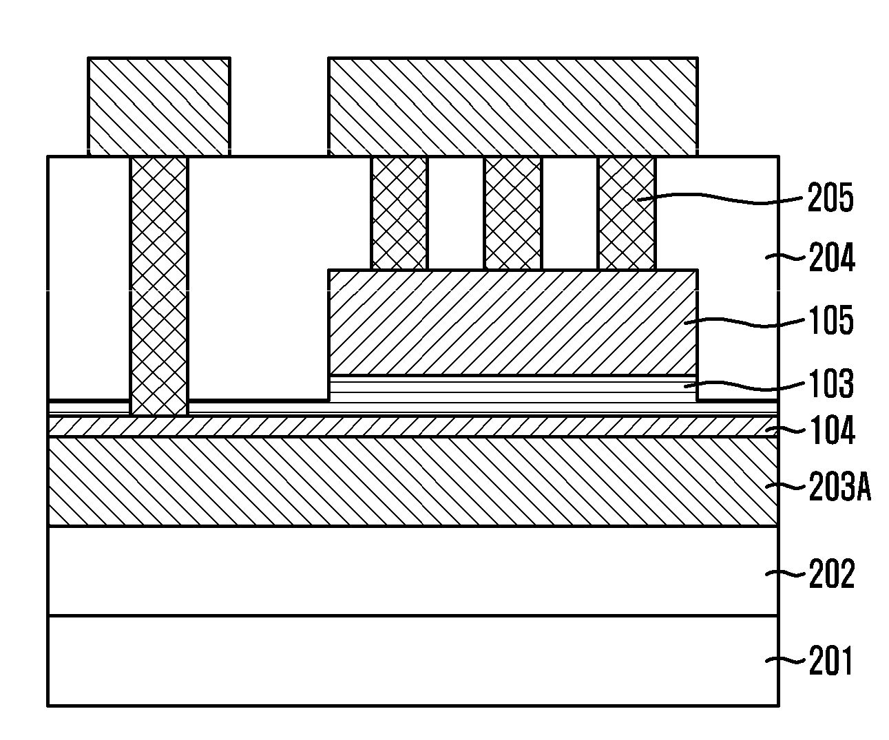
[0074]In implementing a capacitor, the electrostatic capacitance is determined by the dielectric constant and the thickness of an insulator and the I-V characteristics are determined by the material and the thickness of the insulator. This, however, is possible only when other processes are implemented stably in the capacitor fabrication process. In implementing the capacitor, the important process is a process of etching a second electrode 105 (i.e., a top electrode) as illustrated in FIG. 5C.

[0075]FIG. 11 is a graph illustrating the I-V characteristics of a capacitor that is fabricated by leaving an insulator on a first electrode 104 (i.e., a bottom electrode) (split1) or removing all of the insulator (split2) when etching a second electrode 105.

[0076]As can be seen from FIG. 11, a leakage current is high in the split 2 than in the split 1. This is because a metallic polymer, which was formed when a portion of the first electrode 104 was etched, adheres to the side of the capacito...


PUM

PropertyMeasurementUnit
Temperatureaaaaaaaaaa
Fractionaaaaaaaaaa

Abstract

Disclosed is a multilayer insulator, a metal-insulator-metal (MIM) capacitor with the same, and a fabricating method thereof. The capacitor includes: a first electrode; an insulator disposed on the first electrode, the insulator including: a laminate structure in which an aluminum oxide (Al2O3) layer and a hafnium oxide (HfO2) layer are laminated alternately in an iterative manner and a bottom layer and a top layer are formed of the same material; and a second electrode disposed on the insulator.

Description

CROSS-REFERENCE TO RELATED APPLICATIONS[0001]The present invention claims priority of Korean Patent Application No. 10-2008-0100228, filed with Korean Intellectual Property Office on Oct. 13, 2008, which is incorporated herein by reference.BACKGROUND OF THE INVENTION[0002]1. Field of the Invention[0003]The present invention relates to semiconductor fabrication technology; and, more particularly, to a multilayer insulator, a metal-insulator-metal (MIM) capacitor with the same, and a fabricating method thereof.[0004]2. Description of Related Art[0005]A capacitor with a MIM structure (hereinafter referred to as an MIM capacitor) is widely used in analog and radio frequency (RF) circuits. Recently, a demand for a high electrostatic capacitance has increased rapidly for the fabrication cost reduction and the high integration of a semiconductor device. Also, it is essential to develop a capacitor with good leakage current characteristics for use in a high-sensitive application device. The...

Claims


Application Information

Patent Timeline
IPC IPC(8): H01G4/06H01L21/02B32B9/00B32B7/02B32B37/02C23C16/44
CPCB32B37/02Y10T428/2495B32B2311/24B32B2457/00H01G4/33H01L21/02178H01L21/02181H01L21/022H01L21/02274H01L21/0228H01L21/3142H01L28/40Y10T428/26Y10T156/10B32B2311/00H01L2924/0002H01L2924/00H10B99/00H10B12/00H01L21/768H01L21/3213H01L23/5226H01L23/5223H01L23/528H01L21/31111H01L21/7684H01L21/28556H01L23/53214H01L21/02107
Inventor KIM, KWAN-SOOKIM, SOON-WOOK
Owner KEY FOUNDRY CO LTD
Why Eureka
Try Eureka