Semiconductor Optical Device and Manufacturing Method Thereof

a technology of semiconductors and optical devices, which is applied in the direction of optical elements, semiconductor lasers, instruments, etc., can solve problems such as deterioration of transmission properties, and achieve the effects of reducing size, excellent properties, and less chirping

Active Publication Date: 2008-09-11
LUMENTUM JAPAN INC
View PDF6 Cites 24 Cited by
  • Summary
  • Abstract
  • Description
  • Claims
  • Application Information

AI Technical Summary

Benefits of technology

[0005]Generally, for long-distance transmission at a modulation speed of 10 Gbps or higher or generation of high speed signals at a modulation speed of 40 Gbps or higher, external modulation systems with less chirping capable of high speed modulation are adopted. Among all, semiconductor electro adsorption (EA) modulation device utilizing the electro absorption effect has an excellent property in view of the reduced size, less power consump

Problems solved by technology

In the EA/DFB laser, when optical feedback caused by light reflection at light emitting edge is incident aga

Method used


Image

  • Semiconductor Optical Device and Manufacturing Method Thereof
  • Semiconductor Optical Device and Manufacturing Method Thereof
  • Semiconductor Optical Device and Manufacturing Method Thereof

Examples


first embodiment

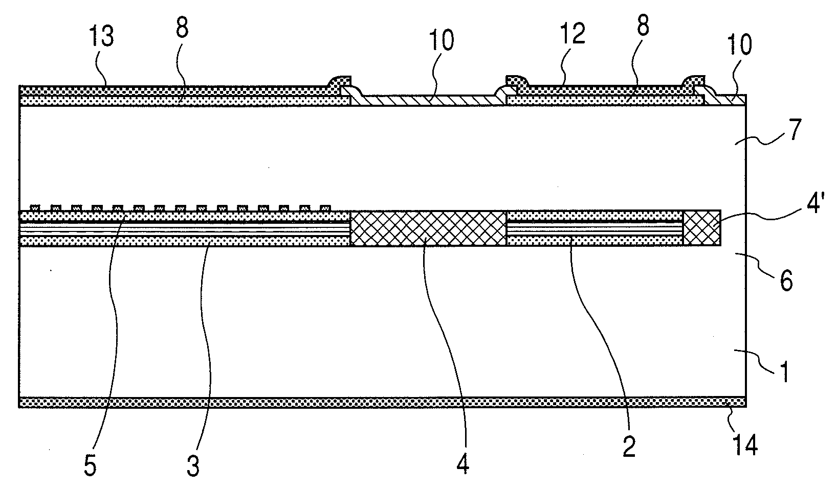
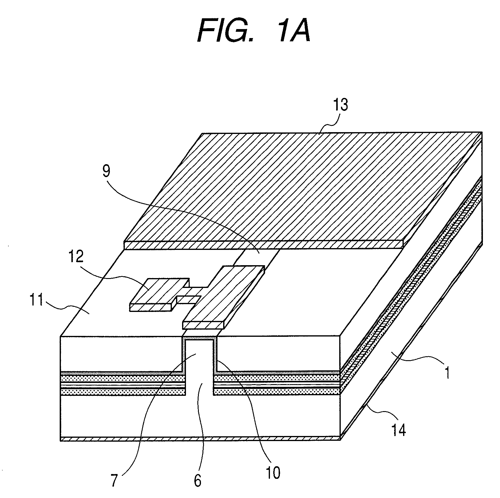
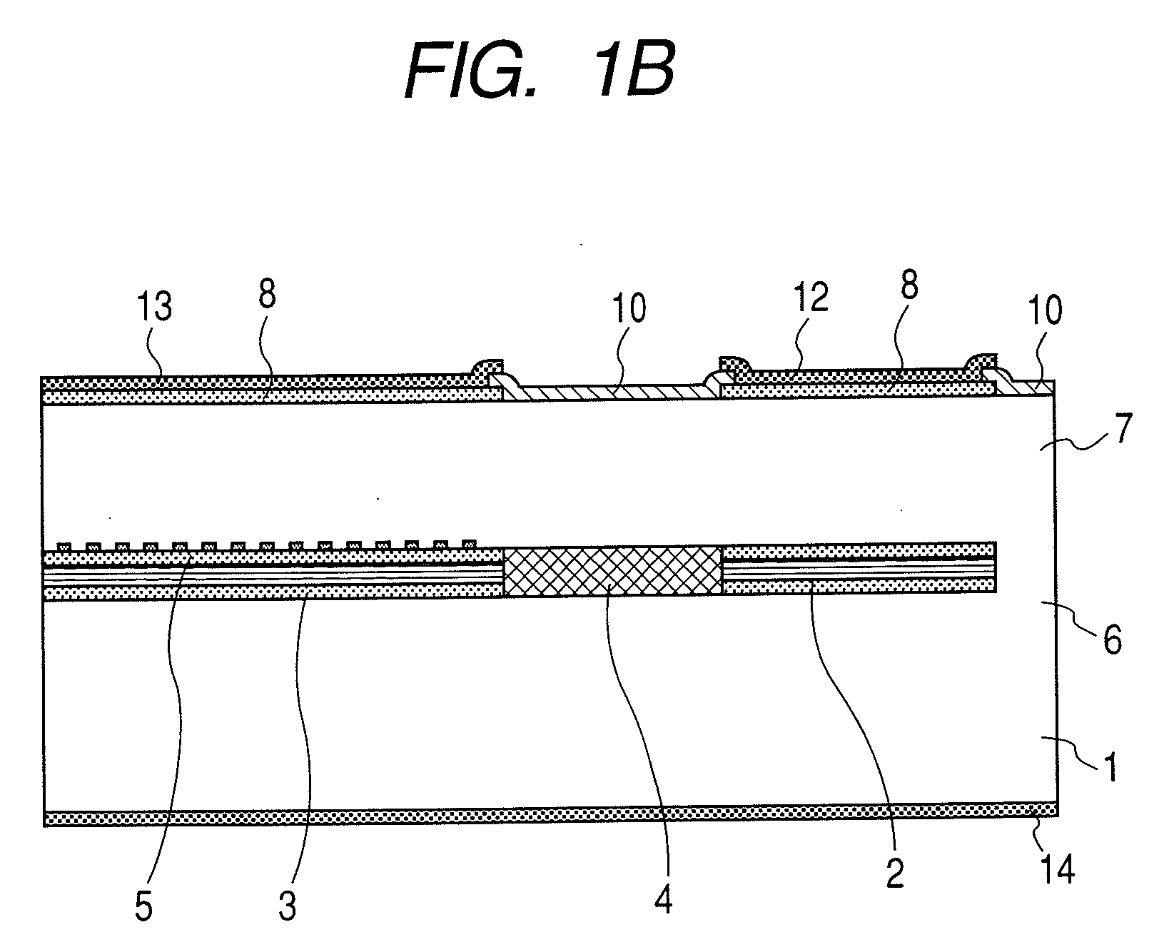
[0046]This embodiment concerns an RWG-EA / DFB(DBR).

[0047]Manufacturing steps of a semiconductor optical integrated device applied with the invention are to be described with reference to FIG. 5.

[0048]However, the drawings are only for description of this embodiment and the size of the drawing and the reduced scale described in this embodiment do not always agree to each other.

[0049]A quantum well structure 2 comprising an InGaAlAs-based material as an electro-absorption optical modulation region is formed by an MOCVD method above an n-InP type substrate 1 (FIG. 5A). For the quantum well structure, an optical confinement structure sufficient for extinction can be formed by alternately stacking quantum wells and barrier layers by about 10 layers. Successively, etching is conducted as far as the surface of the n-InP substrate 1 while leaving a predetermined length of an electro-absorption optical modulator (FIG. 5B). Further, the etching technique for the semiconductor layer having In, ...

second embodiment

[0062]In the ridge waveguide type semiconductor optical integrated device described in the first embodiment, the optical feed back at the light emitting edge can be further decreased by forming a curved waveguide 9′ having an optical axis thereof in a curved shape from the vicinity of the junction portion between the semiconductor laser portion 3 and the optical waveguide 4 to the light emitting edge upon forming the mesa waveguide 9 described in FIG. 5I. FIG. 6 shows a perspective view of a curved waveguide type semiconductor optical integrated device. Since the method of manufacturing the curved waveguide type semiconductor optical integrated device is not different at all from the method described for FIG. 5A to FIG. 5L except for the shape of the waveguide 9′ formed in FIG. 5I as described above, detailed description is to be omitted.

[0063]Further, since the operation method of the curved waveguide type semiconductor integrated device described in the second embodiment is not di...

third embodiment

[0064]This embodiment concerns a BH type EA / DFB(DBR).

[0065]FIG. 7A shows a perspective view and FIG. 7B shows a perspective view showing a cross section taken along a central portion according to an embodiment of a semiconductor optical integrated device applied with the invention.

[0066]In this case, the drawing for the manufacturing step of the device shown in FIG. 5 of the first embodiment is to be omitted.

[0067]However, the drawings are only for description of this embodiment and the size of the drawing and the reduced scale described in this embodiment do not always agree to each other.

[0068]A quantum well structure 2 comprising an InGaAlAs-based material as an electro-absorption optical modulator is formed by an MOCVD method above an n-InP type substrate 1. For the quantum well structure, an optical confinement structure sufficient for extinction can be formed by alternately stacking quantum wells and barrier layers by about 10 layers. Successively, etching is conducted as far ...


PUM


Abstract

A low reflective window structure in an existent electro-absorption optical modulator involves a trading off problem between the increase in the parasitic capacitance and the pile-up. This is because the capacitance density of the pn junction in the window structure is higher compared with the pin junction as the optical absorption region, and the application of electric field to the optical absorption region becomes insufficient in a case of receding the electrode structure from the junction between the optical absorption region and the window structure making it difficult to discharge photo-carriers generated in the optical absorption region. An undope waveguide structure comprising a structure having such compositional wavelength and a film thickness that the compositional wavelength for each of multi-layers constituting the waveguide structure is sufficiently shorter than that of the signal light and the average refractive index is about identical with that in the optical absorption region may be disposed. In a case of forming the electrode structure so as to overlap the junction boundary between the optical absorption region and the undope waveguide, and do not extend on the joined boundary between the undope waveguide and the window structure, increase in the parasitic capacitance due to the pn junction of the window structure and pile up can be suppressed simultaneously.

Description

CLAIM OF PRIORITY[0001]The present application claims priority from Japanese Application JP 2007-056538 filed on Mar. 7, 2007, the content of which is hereby incorporated by reference into this application.FIELD OF THE INVENTION[0002]The present invention concerns a semiconductor optical device and a manufacturing method thereof and it particularly relates to a semiconductor optical modulation device and an integrated semiconductor light emitting device formed by integrating the same.BACKGROUND OF THE INVENTION[0003]Along with rapid popularization of broadband networks, it has become an important subject for optical transceiver modules to increase the operation speed, reduce the size and lower the consumption power. In Metro-area optical communication networks that connect between cities and relay stations, it has been demanded to transmit high speed signals at a communication rate of 10 Gbps through long-distance fibers of from 40 km to 80 km without relay. Further, a trend of incr...

Claims


Application Information

Patent Timeline
IPC IPC(8): H01S5/00G02B6/10H01L21/00H01S5/12
CPCB82Y20/00H01S5/02276H01S5/02284H01S5/026H01S5/0265H01S5/34306H01S5/06256H01S5/101H01S5/12H01S5/227H01S5/0425H01L2224/48091H01S5/04256H01S2301/176H01S5/02345H01S5/02251H01L2924/00014
Inventor MAKINO, SHIGEKISHINODA, KAZUNORIKITATANI, TAKESHI
Owner LUMENTUM JAPAN INC
Why Eureka
Try Eureka