Metal-insulator-metal capacitors and methods of forming the same

a technology of metal-insulator and capacitor, which is applied in the direction of capacitors, semiconductor devices, electrical apparatus, etc., can solve the problems of complex structure of capacitors of conventional semiconductor devices, degrade electrical characteristics of mim capacitors, and unstable process environment of semiconductor fabrication processes, so as to simplify semiconductor fabrication processes

Inactive Publication Date: 2006-08-17
SAMSUNG ELECTRONICS CO LTD
View PDF7 Cites 43 Cited by
  • Summary
  • Abstract
  • Description
  • Claims
  • Application Information

AI Technical Summary

Benefits of technology

[0010] Therefore, according to some embodiments of the present invention, there are provided metal-insulator-metal (MIM) capacitors including an etch stop layer pattern and an etch buffer layer disposed on a

Problems solved by technology

Thus, process environments in the semiconductor fabrication processes may be unstable due to the characteristics of the upper and lower electrodes, the dielectric layer pattern, and the layers surrounding the circuit interconnections.
This may degrade

Method used


Image

  • Metal-insulator-metal capacitors and methods of forming the same
  • Metal-insulator-metal capacitors and methods of forming the same
  • Metal-insulator-metal capacitors and methods of forming the same

Examples


Embodiment Construction

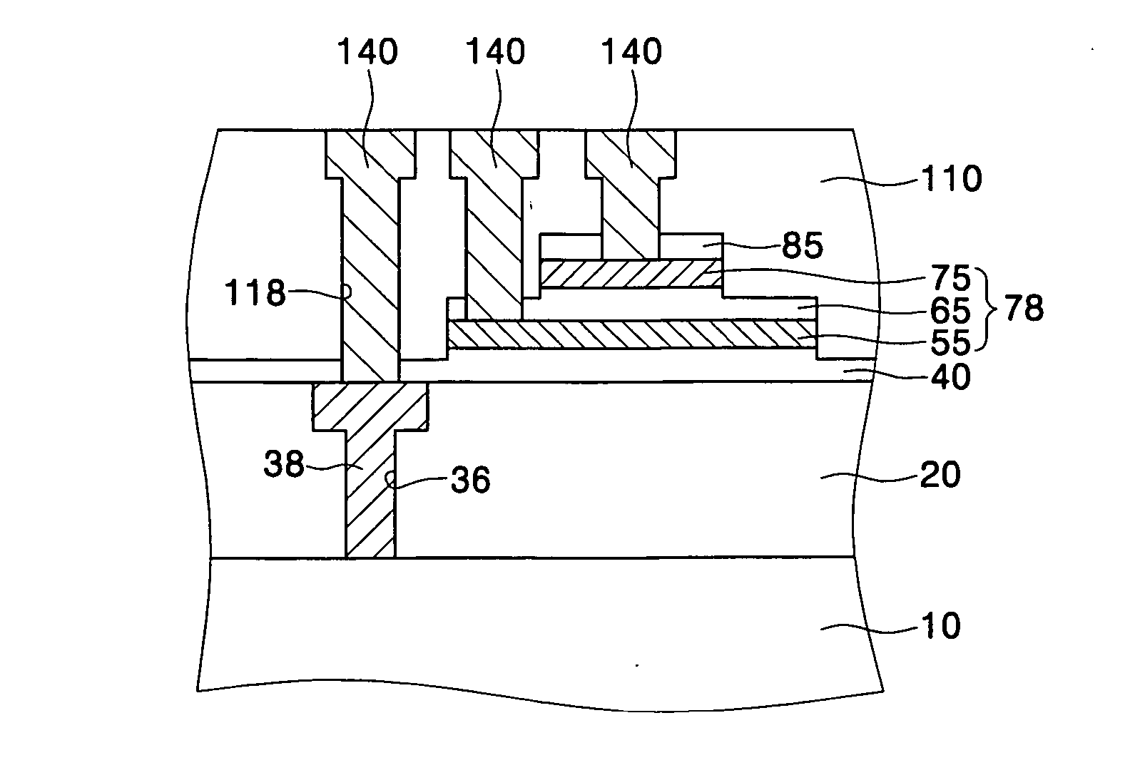
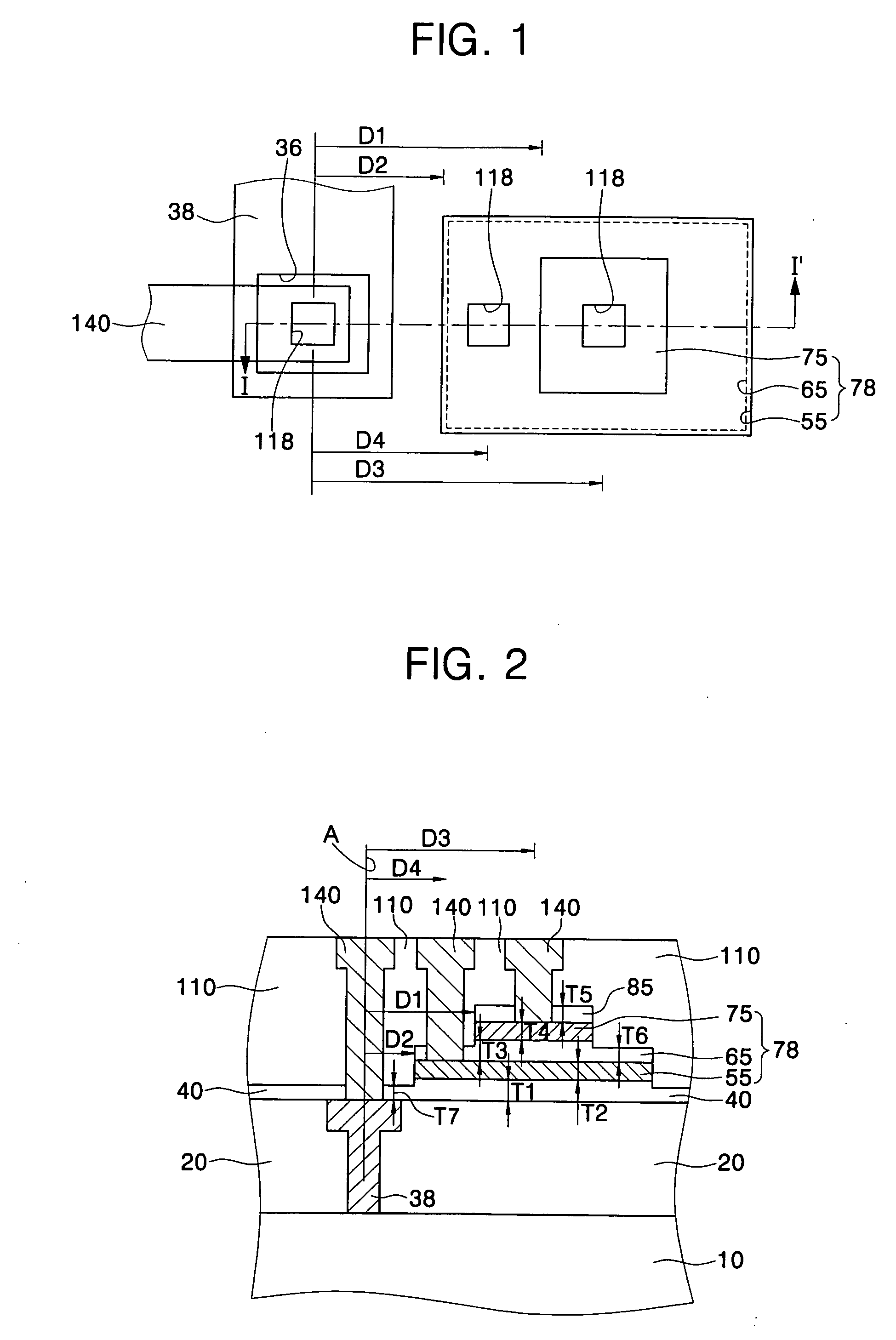
[0019]FIG. 1 is a layout view showing a capacitor according to the present invention, and FIG. 2 is a cross-sectional view showing a capacitor taken along line I-I′ of FIG. 1.

[0020] Referring to FIGS. 1 and 2, an etch buffer layer 40 is disposed on a semiconductor substrate 10. The etch buffer layer 40 has a convex surface on a predetermined region thereof, meaning that the etch buffer layer has a protrusion or higher thickness region. Upper and lower electrodes 75, 55 are sequentially stacked on the convex surface of the predetermined region of the etch buffer layer 40. The upper electrode 75 has a different area than the lower electrode 55. The lower electrode 55 is preferably disposed with an area greater than that of the upper electrode 75. Thus, the lower electrode 55 is disposed to expose a portion of the etch buffer layer 40. A thickness T7 of one portion of the etch buffer layer 40 is different from a thickness T1 of a center portion of the etch buffer layer 40. The thickne...


PUM


Abstract

There are provided metal-insulator-metal (MIM) capacitors and methods of forming the same. The capacitors and the formation methods thereof provide a way of simplifying semiconductor fabrication processes, using component elements of the capacitor and insulating layers around the capacitor. To this end, lower and upper electrodes are sequentially stacked on a semiconductor substrate. A dielectric layer pattern is interposed between the upper and lower electrodes. An etch stop layer pattern and an etch buffer layer are disposed on the upper electrode and under the lower electrode, respectively. The upper and lower electrodes are disposed to expose the dielectric layer pattern and the etch buffer layer.

Description

CROSS-REFERENCE TO RELATED APPLICATION [0001] This patent application claims priority from Korean Patent Application No. 10-2005-0012436, filed Feb. 15, 2005, the contents of which are hereby incorporated by reference in their entirety. BACKGROUND OF INVENTION [0002] 1. Technical Field [0003] The present invention relates to discrete elements of a semiconductor device, and more particularly, to metal-insulator-metal (MIM) capacitors and methods of forming the same. [0004] 2. Discussion of the Related Art [0005] Recently, semiconductor devices have been fabricated to include system-on-chip (SOC) type systems. The SOC has various kinds of semiconductor circuits on a semiconductor substrate. The semiconductor circuits have different functions for data transferring, caching, or the like. Typically, the SOC includes a metal-insulator-metal (MIM) capacitor. The MIM capacitor has higher efficiency in the SOC as compared with a metal-oxide-semiconductor (MOS) capacitor because the MIM capac...

Claims


Application Information

Patent Timeline
IPC IPC(8): H01L21/8242
CPCH01L21/76807H01L21/76816H01L28/60H01L21/31H01L27/04
Inventor LEE, SANG-JINMOON, YOUNG-JOONLEE, SEUNG-KOOLEE, KYUNG-TAE
Owner SAMSUNG ELECTRONICS CO LTD
Why Eureka
Try Eureka