Integration of a MIM capacitor over a metal gate or silicide with high-k dielectric materials

a technology of dielectric materials and integrated circuits, applied in the direction of capacitors, semiconductor devices, electrical equipment, etc., can solve the problem of being unable to integrate mim structures into beol structures

Inactive Publication Date: 2007-03-15
GLOBALFOUNDRIES INC
View PDF10 Cites 36 Cited by
  • Summary
  • Abstract
  • Description
  • Claims
  • Application Information

AI Technical Summary

Benefits of technology

[0009] The introduction of metal gates and HiK dielectric materials creates a demand for advanced passive device integration schemes, which will be needed in the future to complement advanced CMOS. The integration scheme of the present invention eliminates the need for BEOL MIM integration, which will as stated above will eventually be impossible due to the reduction of Via heights. With the integration scheme of the present invention that issue is overcome.
[0013] The advantages uses a metal gate and HiK dielectric to make a MIM capacitor include, first, provision of a capacitor compatible with metal / HiK gate CMOS integration. A second advantage is that the MIM capacitor produced has better linearity as compared to the current MOS capacitors and hence a better RF device is produced. Thirdly, the use of the HiK dielectric layer in the MIM capacitors provides high capacitance density which is suitable for both decoupling and RF capacitors. In addition, there is no need for BEOL MIM integration, which is increasingly difficult with each new generation of integrated circuit devices because of the requirement of reduction of the via height.

Problems solved by technology

However we have observed that it will eventually be impossible to integrate MIM structures into BEOL structures as the heights of Vias are reduced to smaller and smaller dimensions.

Method used


Image

  • Integration of a MIM capacitor over a metal gate or silicide with high-k dielectric materials
  • Integration of a MIM capacitor over a metal gate or silicide with high-k dielectric materials
  • Integration of a MIM capacitor over a metal gate or silicide with high-k dielectric materials

Examples


first embodiment

[0041]FIG. 3A is schematic sectional view of a semiconductor device 301 including a Metal Insulator-Metal (MIM) capacitor 310 in accordance with this invention. The semiconductor device 301 is manufactured according to the process of this invention, as shown by the flow chart of FIG. 3B.

[0042] The Metal Insulator-Metal (MIM) capacitor 310 is formed on a base comprising a semiconductor substrate 31 having a top surface 31T. A Shallow Trench Isolation (STI) region 33 is formed in the region of the surface 31T of the substrate 31. The STI region 33 has a top surface 33T coplanar with the top surface 31T of the semiconductor substrate 31. The MIM capacitor lower plate 38M is a metal electrode formed on the top surface 33T of the STI region 33. A HiK dielectric layer 40 of the MIM capacitor 310 is formed on the top surface 38T of the lower plate 38M of the MIM capacitor 310. The MIM capacitor top plate 42M is formed on the HiK dielectric layer 40 above the lower plate 38M. An etch stop ...

second embodiment

[0056]FIG. 4A is schematic sectional view of a semiconductor device 401 in accordance with this invention including a Metal Insulator-Metal (MIM) capacitor 410. The semiconductor device 401 is manufactured in accordance with the process of this invention which is shown by the flow chart of FIG. 4B.

[0057] As shown in FIG. 4A the MIM capacitor 410 is formed on a base comprising a semiconductor substrate 31 having a top surface 31T with an STI region 33 formed in a region of the surface 31T of the substrate 31. Moreover, also as in FIG. 3A the STI region 33 has a top surface 33T coplanar with the top surface 31T of the semiconductor substrate 31. In the case of FIG. 4A, however, the MIM capacitor 410 has a silicided lower plate 38L. A portion 38P of the silicided lower plate 38L is a conductive (doped) polysilicon layer 38P formed on the top surface 33T of the STI region 33. The complementary portion of the laminated lower plate 38L is a conventional conductive (doped) silicide layer ...

third embodiment

[0071]FIG. 5A is schematic sectional view of a semiconductor device 501 including a Metal Insulator-Metal (MIM) capacitor 510 in accordance with this invention. The semiconductor device 501 is manufactured according to the process of this invention shown by the flow chart of FIG. 5B.

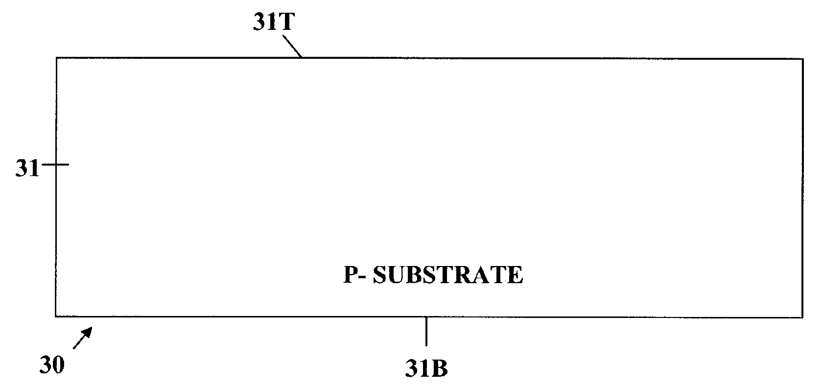
[0072] As shown in FIG. 5A the MIM capacitor 510 is formed on a base comprising a semiconductor substrate 31 having a top surface 31T. A P / N (Positively or Negatively doped) well 35 is formed in a region of the surface 31T of the substrate 31, with the P / N well 35 serving as the lower plate of the MIM capacitor 510. The P / N well 35 has a top surface 35T coplanar with the top surface 31T of the semiconductor substrate 31. A capacitor HiK dielectric layer 160 is formed on the top surface 35T of the P / N well. The top plate 142 of the MIM capacitor 510 is formed on the top surface 160T of the HiK dielectric layer 160 above the doped P / N well 35, i.e. the lower plate of the MIM capacitor 510. An etch stop la...


PUM

PropertyMeasurementUnit
dielectricaaaaaaaaaa
HiK dielectricaaaaaaaaaa
densityaaaaaaaaaa

Abstract

A Metal Insulator-Metal (MIM) capacitor is formed on a semiconductor substrate with a base comprising a semiconductor substrate having a top surface and including regions formed in the surface selected from a Shallow Trench Isolation (STI) region and a doped well having exterior surfaces coplanar with the semiconductor substrate. An ancillary MIM capacitor plate is selected either a lower electrode formed on the STI region in the semiconductor substrate or a doped well formed in the top surface of the semiconductor substrate. A capacitor HiK dielectric layer is formed on or above the MIM capacitor lower plate. A second MIM capacitor plate is formed on the HiK dielectric layer above the MIM capacitor lower plate.

Description

BACKGROUND OF THE INVENTION [0001] This invention relates to a method for making a capacitor structure for high-density integrated circuits and the structure produced thereby, and more particularly relates to a method for making a Metal Insulator-Metal (MIM) capacitor having a HiK dielectric constant and the structure produced thereby. [0002] In the semiconductor industry, currently there is a trend towards the use of metal gates for CMOS and HiK dielectric materials in high-density integrated circuit devices. This trend is based on the need to employ metal gates to reduce the problem of high leakage currents that result from device scaling to smaller and smaller dimensions as tox (thickness of silicon oxide) is reduced as the silicon oxide is thinned down for constant field scaling. [0003] In industry, MIM capacitors are used in integrated circuits, especially those integrated circuits used in Radio Frequency (RF) and other high-frequency applications. The requirement for high capa...

Claims


Application Information

Patent Timeline
Patent Type & Authority Applications(United States)
IPC IPC(8): H01L29/00
CPCH01L28/40
Inventor CHINTHAKINDI, ANIL KUMARCOOLBAUGH, DOUGLAS DUANEDOWNES, KEITH EDWARDESHUN, EBENEZER E.HE, ZHONG-XIANGRASSEL, ROBERT MARKSTAMPER, ANTHONY KENDALLVAED, KUNAL
Owner GLOBALFOUNDRIES INC
Why Eureka
Try Eureka