Eureka AIR delivers breakthrough ideas for toughest innovation challenges, trusted by R&D personnel around the world.

Memory arrangement with low power consumption

Active Publication Date: 2006-06-08
INFINEON TECH AG
View PDF6 Cites 0 Cited by
  • Summary
  • Abstract
  • Description
  • Claims
  • Application Information

AI Technical Summary

Benefits of technology

[0016] Because the supply voltage line is shorter than the result line, a coupling capacitance between the supply voltage line and the result line is less than if the supply voltage line was as long as the result line, as is in the prior art. Additionally, for the same reason, the inherent capacitance of the supply voltage line according to the invention is less than the inherent capacitance according to the prior art would be. By reducing the coupling capacitance, a restoration period, which allows the result line to again accept a different supply voltage potential from the supply voltage line, is also shortened. In this way, a switching time of the memory arrangement is also reduced, and a maximum clock rate of the memory arrangement is increased. Additionally, by reducing the coupling capacitance and inherent capacitance, a power consumption to charge the supply voltage line onto a supply voltage potential is reduced.
[0023] Since by activating a word line and a supply voltage line, two bits are read simultaneously, an area of a memory arrangement can be reduced in comparison with an otherwise similar memory arrangement in which when a word line and a supply voltage line are activated only one bit is read.

Problems solved by technology

In addition to the negative effect on the clock rate of the ROM 8, the coupling capacitance has a negative effect on the power consumption of the ROM 8.
Additionally, there is a negative effect on the power consumption by the inherent capacitance of each virtual supply voltage line 1, which must be charged onto the second supply voltage at a read operation.

Method used


Image

  • Memory arrangement with low power consumption
  • Memory arrangement with low power consumption
  • Memory arrangement with low power consumption

Examples


Embodiment Construction

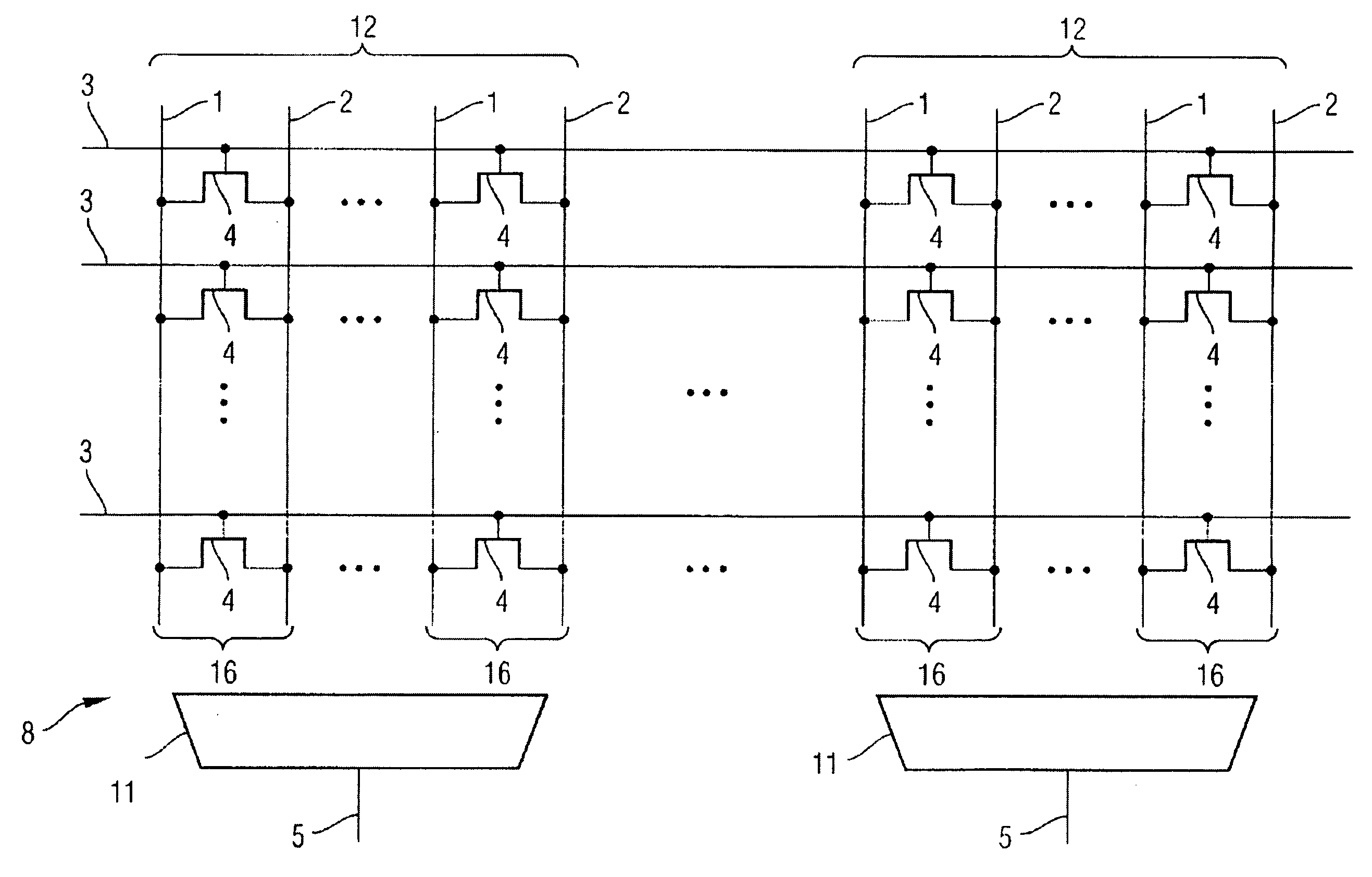
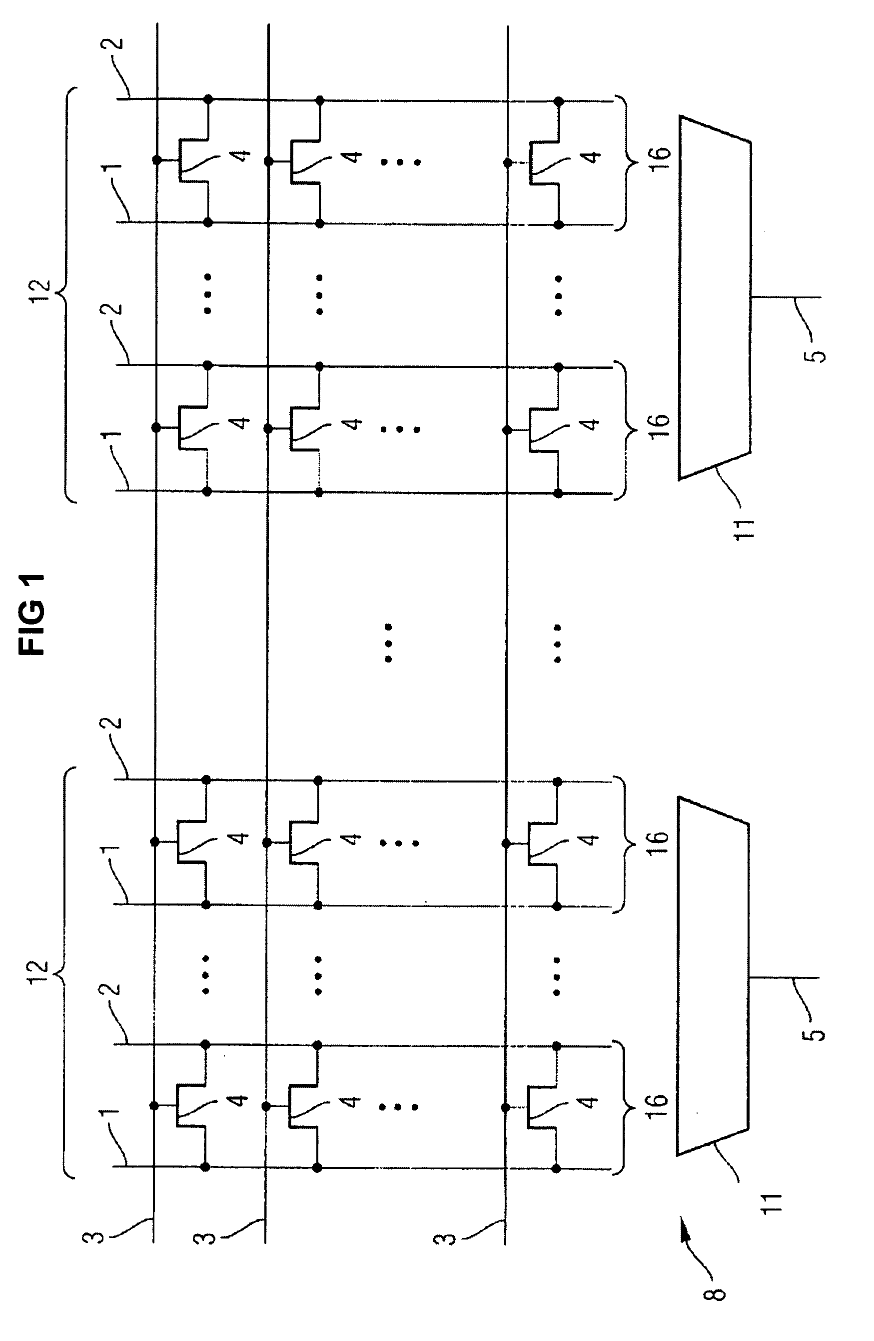
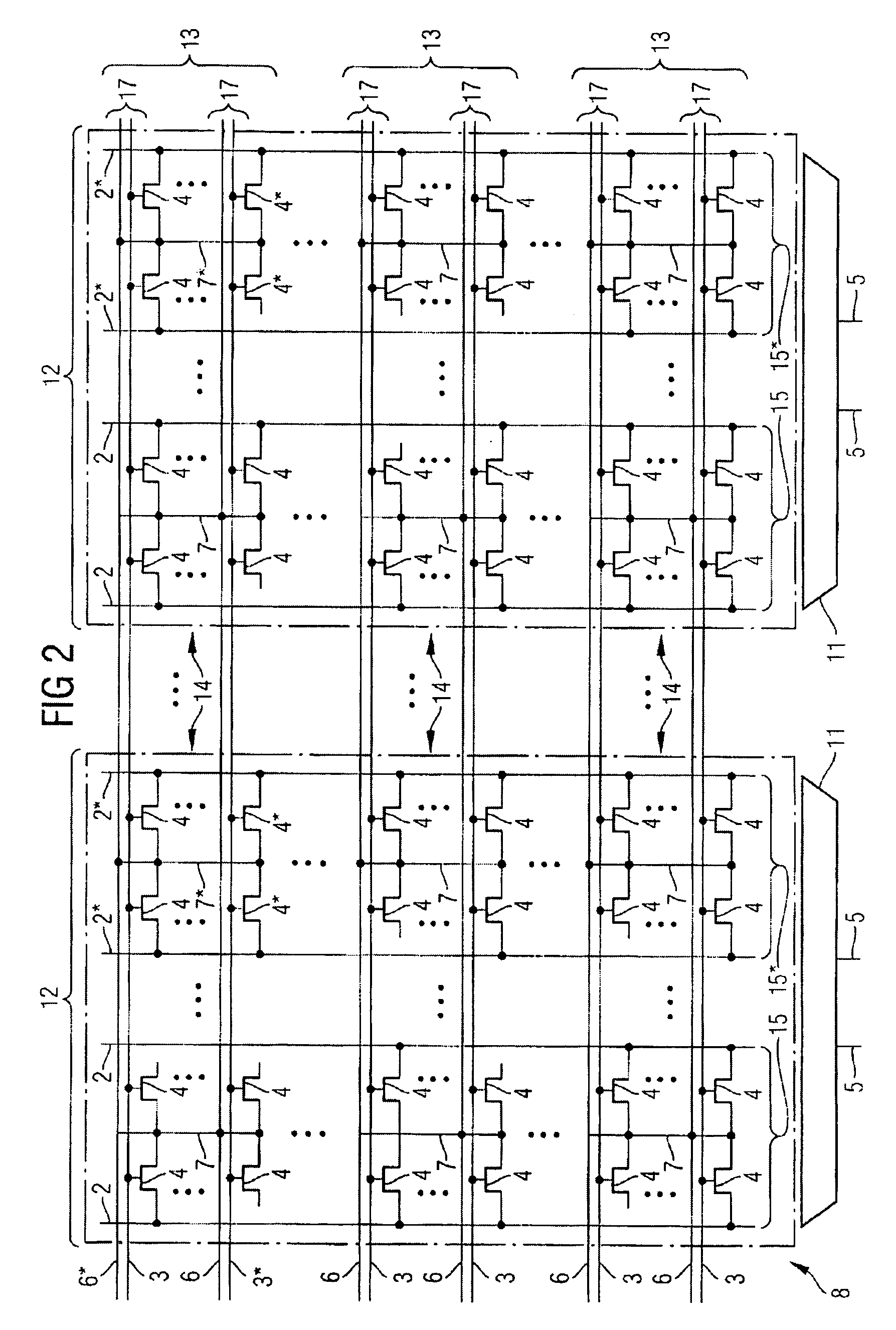
[0034] Identical or functionally identical elements and signals are referred to with the same reference symbols in the figures of the drawing unless stated otherwise.

[0035] In FIG. 2, a ROM 8 according to the invention, consisting of multiple blocks 14, is shown. A specified number of blocks 14 forms a block column 12, two of which are shown. Similarly, n / 2 blocks form a block row 13, three of which are shown. The reference n stands for a word width of a data item which is read out of the ROM 8 in a read operation. Each word line 3 and also each further supply voltage line or global virtual supply voltage line 6 runs through the whole width of the ROM8 or each double column 15 of the ROM 8. Each bit line 2 of the ROM 8 runs through the whole length of the ROM 8 or each row 17 of the ROM 8. On the other hand, each supply voltage line or local virtual supply voltage line 7 runs through only the length of a block 14 of the ROM 8. Each global virtual supply voltage line 6 is connected ...


PUM


Abstract

A memory arrangement, particularly a ROM, having memory cells, local virtual supply voltage lines, word lines and result lines may also include global virtual supply voltage lines that run along the width of the memory arrangement parallel to the word lines. The local virtual supply voltage lines run parallel to the result lines, and perpendicularly to the word lines where the each local virtual supply voltage line runs only within a block of the memory arrangement. Each global virtual supply voltage line, in each block through which it runs, is connected to one local virtual supply voltage line. The coupling capacitance between the supply voltage lines and the result lines, and the inherent capacitance of the supply voltage lines are reduced, reducing the power consumption and increasing the clock frequency of the memory arrangement.

Description

PRIORITY AND CROSS REFERENCE TO RELATED APPLICATION [0001] This application claims priority to German Patent Application No. 10 2004 052 218.9, filed Oct. 27, 2004, which is incorporated by reference herein in its entirety. BACKGROUND OF THE INVENTION [0002] 1. Field of the Invention [0003] This invention relates to memory arrangements such as a read only memory (“ROM”), and in particularly to a memory arrangement having reduced power consumption. [0004] 2. Description of the Related Art [0005]FIG. 1 illustrates a prior art read-only memory (ROM) 8 having many 1-bit memory cells, corresponding to the memory capacity of the ROM. These 1-bit memory cells are divided into various sections (also called block columns below) of equal size (equal number of 1-bit memory cells), depending on a word length of an output data item of the ROM. In each section, the 1-bit memory cells are arranged in columns and rows. A word line 3 of the ROM runs along the same row in all sections of the ROM. On ...

Claims


Application Information

Patent Timeline
IPC IPC(8): H02M7/04
CPCG11C5/063G11C17/12
Inventor GUPTA, SIDDHARTHMARTELLONI, YANNICK
Owner INFINEON TECH AG
Why Eureka
Eureka Blog
Learn More