Determining film stress from substrate shape using finite element procedures

a technology of finite element and substrate shape, applied in the direction of force/torque/work measurement apparatus, instruments, simultaneous indication of multiple variables, etc., can solve the problems of device failure due to film stress, failure of electronic devices formed on the substrate, low-distortion lithography mask, etc., to accurately determine the film stress

Active Publication Date: 2006-06-15
WISCONSIN ALUMNI RES FOUND
View PDF10 Cites 23 Cited by
  • Summary
  • Abstract
  • Description
  • Claims
  • Application Information

AI Technical Summary

Benefits of technology

[0025] The assumption that the film stress is uniform, or the deformed substrate shape is spherical, is fundamental for applying Stoney's equation, but it is unnecessary for performing a finite element analysis in accordance with the present invention. Thus, the present invention can be used to accurately determine film stress for a film-substrate system in which the curvature, mismatch strain, and film stress are functions of location and direction.

Problems solved by technology

Failure to control these stresses can lead to failure of the electronic devices formed on the substrate.
Device failure due to film stress may be caused, for example, by dislocation generation, film cracking, delamination, and / or void formation.
Design and implementation of a low-distortion lithography mask is one of the key issues for all NGL technologies.
Intrinsic film stress generated during the fabrication process of advanced NGL masks can cause significant mechanical distortions, which compromise the accuracy of image resolution and placement.
However, the equipment required to obtain such direct measurements is expensive, and such methods are not well suited for production environments.
Although most available measuring tools provide accurate information about the induced substrate shape, i.e., the distorted shape of the substrate wafer with film applied, the film stress magnitudes and distributions generated by such techniques, in general, are not reliable.
This is due to the fact that the calculations are based upon the local application of Stoney's equation, which is not valid for most real film-substrate systems.
Thus, when the film is deposited onto the substrate, lattice and thermal mismatch strains are generated.
However, the validity of locally applying Stoney's equation has not been established.
In most cases, the deformed substrate shape is not perfectly spherical, so the applicability of Stoney's equation is significantly limited.
However, in semiconductor and similar device manufacturing cases, the loading, intrinsic stress, or mismatch strain (which causes the film and substrate deformation) is unknown.

Method used


Image

  • Determining film stress from substrate shape using finite element procedures
  • Determining film stress from substrate shape using finite element procedures
  • Determining film stress from substrate shape using finite element procedures

Examples


Embodiment Construction

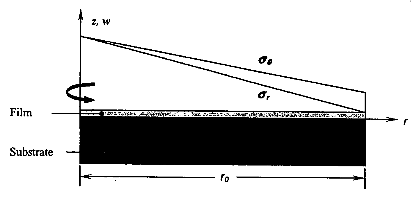
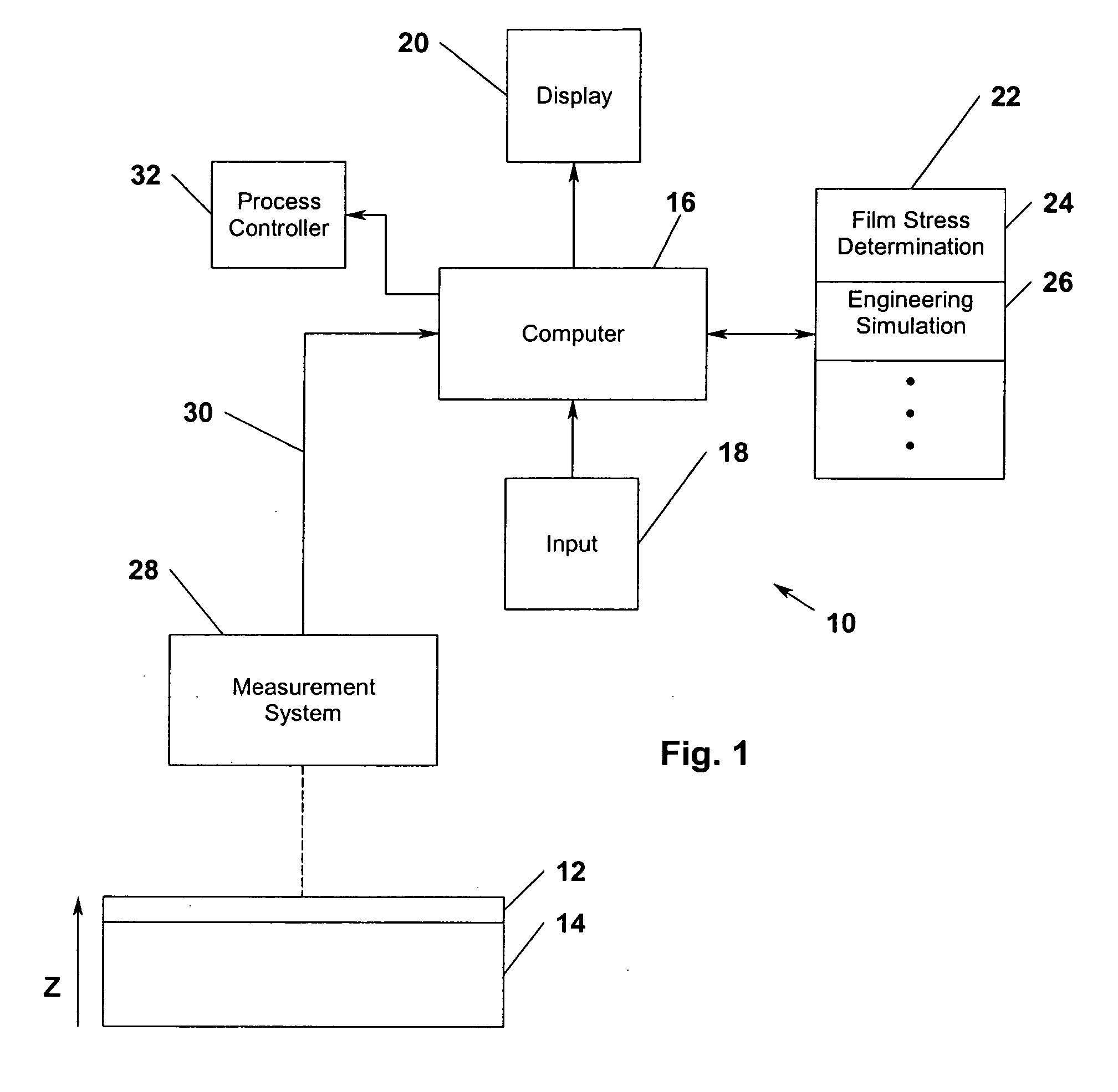
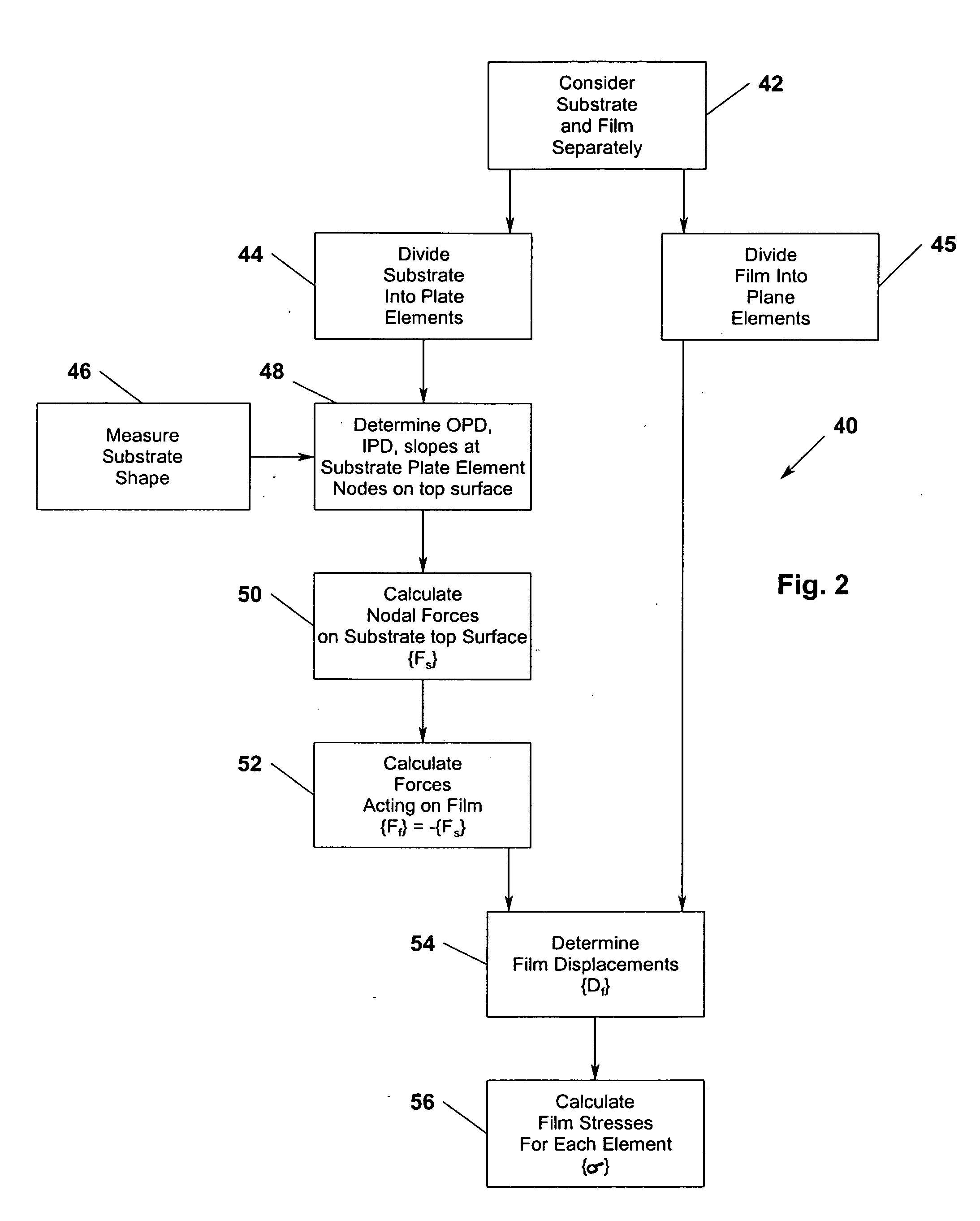
[0032] The present invention now will be described in detail. First, a generic system and method for determining film stress from substrate shape using finite element procedures in accordance with the present invention will be described in detail. An exemplary application of a method for determining film stress from substrate shape using finite element procedures in accordance with the present invention will then be presented in detail. Finally, an exemplary analysis showing the improved accuracy provided by a method for determining film stress from substrate shape using finite element procedures in accordance with the present invention over existing methods for determining film stress using Stoney's equation will be presented. Based on the detailed written description, drawings, and examples provided herein any person skilled in the art to which this invention pertains will be able to implement a method for determining film stress from substrate shape using finite element procedure...


PUM

PropertyMeasurementUnit
thicknessaaaaaaaaaa
compressiveaaaaaaaaaa
stressaaaaaaaaaa

Abstract

A method for determining the stresses in a film applied to a substrate from measured substrate shape. The substrate is first analyzed using finite element techniques to obtain nodal forces at the surface of the substrate to which the film is applied, based on measured distortion data of the substrate surface. The film is then analyzed to calculate the film stresses from the applied nodal forces using finite element techniques. The invention may be applied to determine stresses in thin films applied to a variety of substrates, including those used for micro-electronic (e.g., integrated circuit) and micro-mechanical devices and / or for the lithography masks or other optical / projection systems used to fabricate such devices.

Description

[0001] This application claims the benefit of U.S. Provisional Patent Application No. 60 / 617,970, filed on Oct. 12, 2004.[0002] This invention was made with United States government support awarded by the following agencies: DOD ARPA DAAD17-99-C-0085. The United States has certain rights in this invention.FIELD OF THE INVENTION [0003] This invention pertains generally to systems and methods for analyzing the stress in thin films applied to substrates and, more particularly, to such systems and methods as may be used to analyze thin films as applied to substrates as used in integrated circuit and similar micro-electronic and micro-mechanical device fabrication. BACKGROUND OF THE INVENTION [0004] In the fabrication of integrated circuits, and other semiconductor devices, a substrate wafer, made of a material such as single crystal silicon, is doped, and a thin film is applied on the substrate surface. Thin films of conductive or insulative material may be deposited or otherwise applie...

Claims


Application Information

Patent Timeline
Patent Type & Authority Applications(United States)
IPC IPC(8): G01N3/00
CPCG01L5/0047
Inventor LOVELL, EDWARD G.FENG, ZHAOHUAENGELSTAD, ROXANN L.
Owner WISCONSIN ALUMNI RES FOUND
Why Eureka
Try Eureka