Organic-inorganic composite insulating material for electronic element, method of producing same and field-effect transistor comprising same

a technology of composite insulating materials and electronic elements, which is applied in the direction of thermoelectric device junction materials, electrical apparatus, and semiconductor devices. it can solve the problems of difficult to meet all the aforementioned requirements, insulating films made of inorganic materials with high dielectric constants but lack of flexibility, and insulating films made of phenolic resins exhibit relatively high dielectric constants

Inactive Publication Date: 2006-06-29
FUJIFILM BUSINESS INNOVATION CORP
View PDF10 Cites 23 Cited by
  • Summary
  • Abstract
  • Description
  • Claims
  • Application Information

AI Technical Summary

Benefits of technology

The patent describes a field-effect transistor that uses an insulated gate film made of an organic-inorganic composite insulating material. The volume ratio of the organic polymer in the insulating film should fall within a range of 10%-30%. The transistor is prepared by sequentially laminating a gate electrode, insulated gate film, transporting layer, source electrode, and drain electrode on a substrate. The technical effect of this invention is to provide a more efficient and reliable insulated gate film for field-effect transistors, which can improve the performance and reliability of electronic devices that use these transistors.

Problems solved by technology

The technical problem addressed in this patent is the development of an insulating film for organic thin film transistors (OTFTs) that meets all the requirements of flexibility, high dielectric constant, high insulation resistance, chemical resistance, and low temperature heat treatment. Most existing insulating films made of inorganic materials have limitations in terms of flexibility and chemical resistance, while organic polymers have high dielectric constant but lack chemical resistance. Therefore, there is a need for a new insulating film that can overcome these limitations and provide better performance for OTFTs on flexible substrates.

Method used


Image

  • Organic-inorganic composite insulating material for electronic element, method of producing same and field-effect transistor comprising same
  • Organic-inorganic composite insulating material for electronic element, method of producing same and field-effect transistor comprising same
  • Organic-inorganic composite insulating material for electronic element, method of producing same and field-effect transistor comprising same

Examples


example 1

[0071] The aforementioned coating solution for PVPh-dried alumina gel insulating film is dropped in an amount of 2 ml onto a PEN film (thickness: 125 μm) over which it is then spread by a spin coating method at 4,000 rpm. Thereafter, the coated material is heated to 90° C. over a hot plate in the atmosphere for 1 hour. Subsequently, the coated material is heated to 180° C. in a nitrogen atmosphere for 2 hours to form an organic-inorganic composite insulating material comprising PVPh-dried alumina gel insulating material (thickness: 500 nm; volume ratio of PVPh in the film: 30%).

example 2

[0072] An insulating film is formed in the same manner as in Example 1 except that as the coating solution for insulating film there is used a coating solution for PVPh-dried titania gel insulating film instead of coating solution for PVPh-dried alumina gel insulating film. Thus, an organic-inorganic composite insulating material comprising PVPh-dried titania gel insulating material (thickness: 400 nm; volume ratio of PVPh in the film: 30%) is formed.

example 3

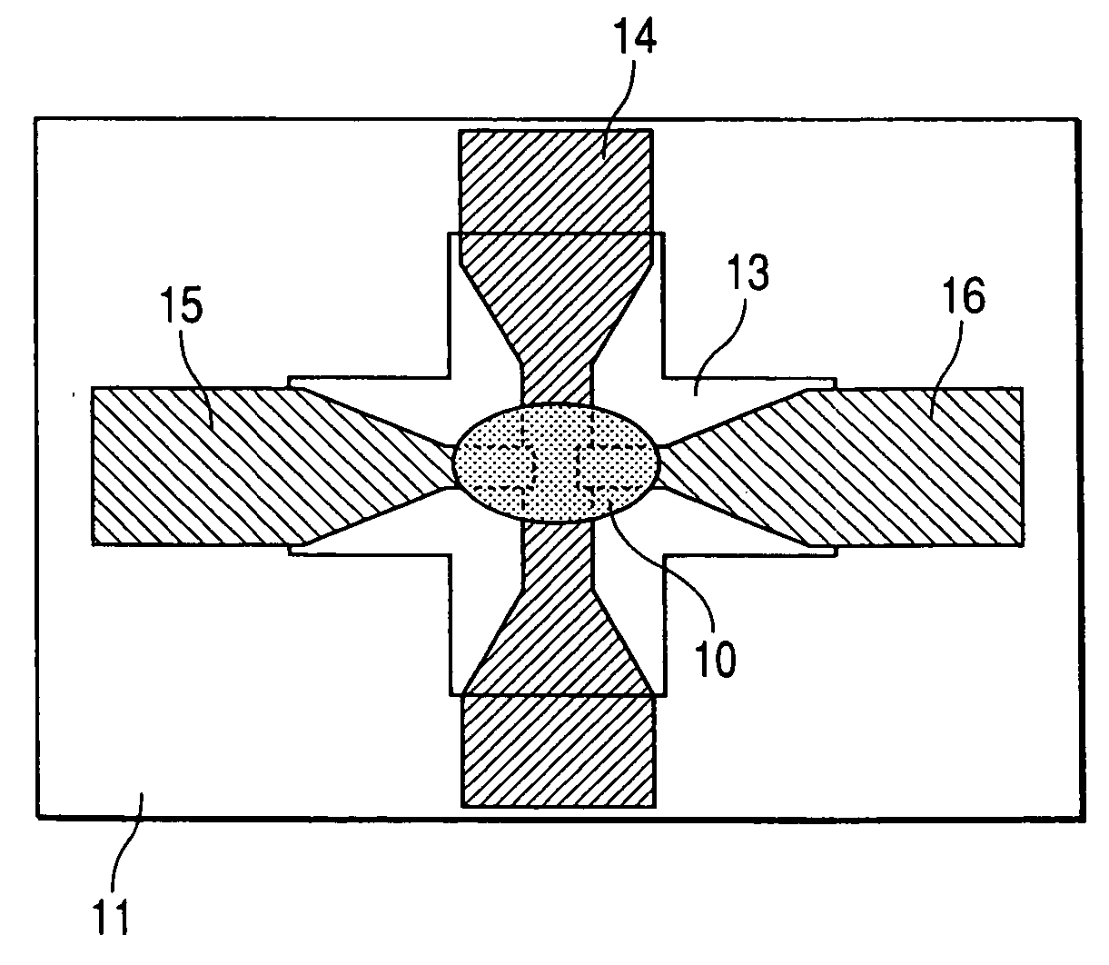
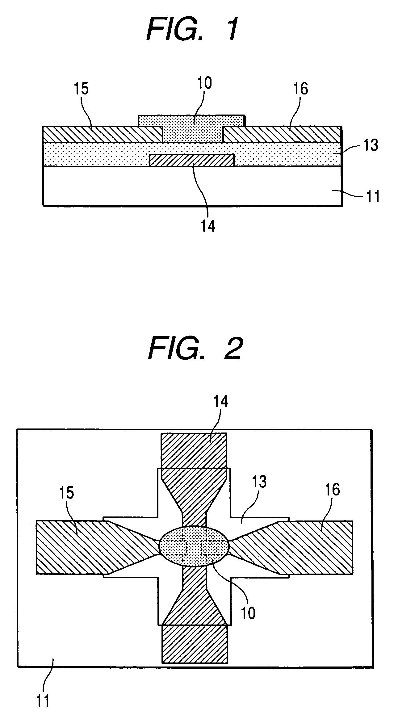
[0086] Field-effect transistors (TFT) according to embodiments shown in FIGS. 1 and 2 comprising a PVPh-dried alumina gel composite film formed in the same manner as in Example 1 as an insulated gate film 13 are prepared.

[0087] As the transporting layer 10 there is used a semiconductive glycerin crosslinked film of carbon nanotube. As the gate electrode 14 there is used aluminum / gold. As the source electrode 15 and the drain electrode 16 there are each used titanium / gold. In this arrangement, a contact with the transporting layer 10 is formed. As the substrate 11 there is used a PEN film (thickness: 125 μm) which is a flexible substrate.

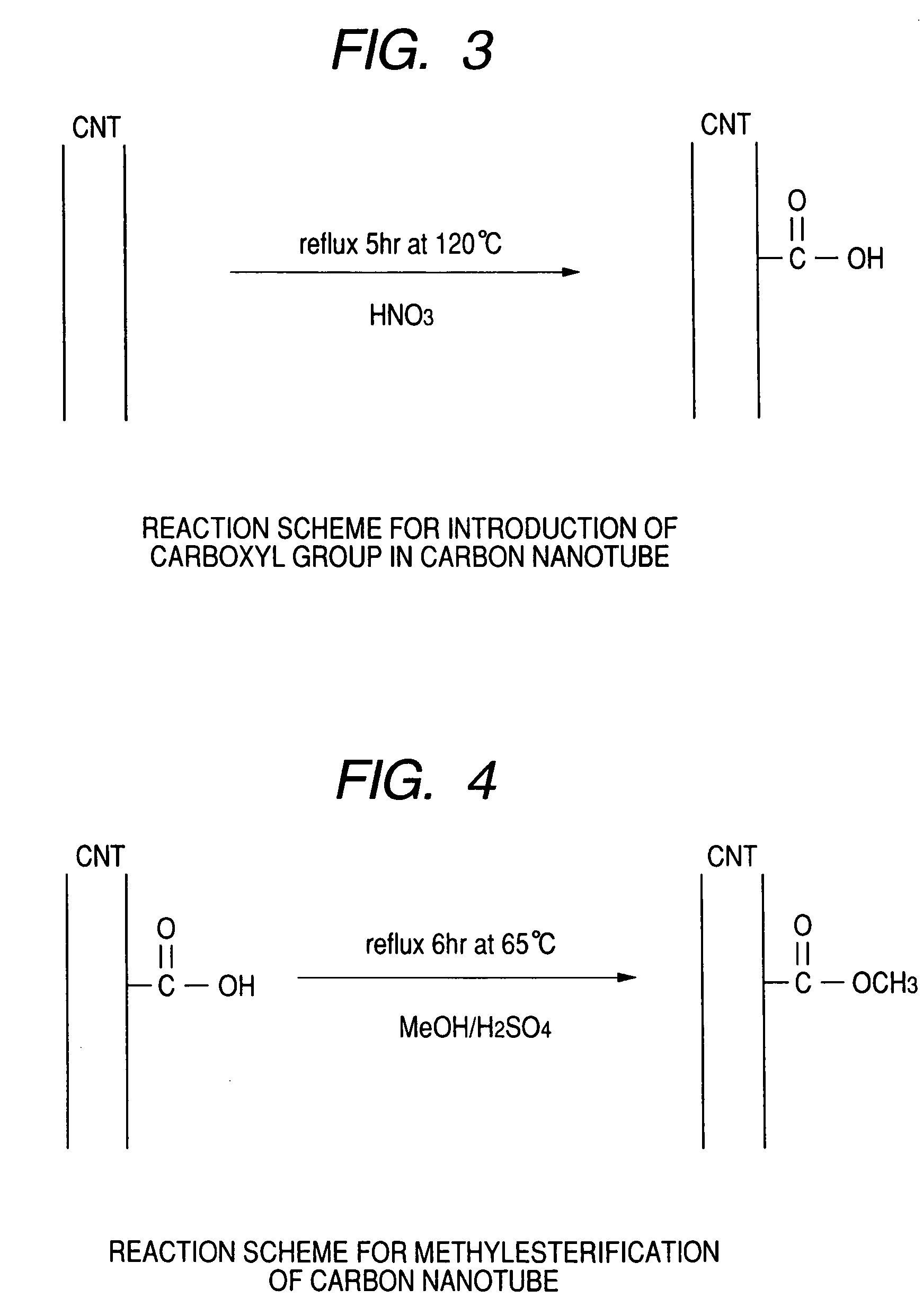
(1) Purification of Single Layer Carbon Nanotube

[0088] 30 mg of a powder (average particle diameter: 1.5 nm; average length: 2 μm) obtained by sifting a single layer carbon nanotube powder (purity: 40%, produced by Aldrich Inc.) through a sieve (pore diameter: 125 μm) to remove coarse agglomerates is heated to 450° C. in a muffle furnace for 15 m...


PUM


Abstract

A method of producing an organic-inorganic composite insulating material for electronic element comprises subjecting a mixture of an organic polymer or its solution and a metal alkoxide or its solution as a starting material to sol-gel reaction of the metal alkoxide in the presence of the organic polymer.

Description


Claims


Application Information

Patent Timeline
Owner FUJIFILM BUSINESS INNOVATION CORP
Why Eureka
Try Eureka