Microelectronic device and method for label-free detection and quantification of biological and chemical molecules

a micro-electronic device and label-free technology, applied in the field of micro-electronic devices and methods for label-free detection and quantification of biological and chemical molecules, can solve the problems of labor-intensive use of such labeling reagents, prone to human and equipment errors, and use of labeling reagents, so as to improve the conductivity of the active channel and widen the scope of practical and worthwhile utilization.

Inactive Publication Date: 2002-01-31
THE UNITED STATES OF AMERICA AS REPRESENTED BY THE SECRETARY OF THE NAVY
View PDF0 Cites 100 Cited by
  • Summary
  • Abstract
  • Description
  • Claims
  • Application Information

AI Technical Summary

Benefits of technology

0016] Another aspect of the invention provides for a method for detecting a target molecule species by contacting the sensor of the present application with a sample solution, which creates an interface between the sample solution and the receptor-modified dielectric layer. The binding of target molecules to the receptor molecules immobilized on the dielectric layer changes the interfacial capacitance that exists between the sample solution and the receptor modified dielectric layer. This change of interfacial capacitance changes the conductivity of the active channel. The conductivity of the active channel modulates an externally supplied current flowing through the active channel when a terminal bias is applied between the source and the drain. The modulation of the externally supplied current flowing through the active channel can be measured to detect binding of the target molecules to the molecular receptors. The methods and devices of the invention remove the dependency of molecular-recognition-based sensors on labeling reagents, which enables a wider scope of practical and worthwhile utilization of recognition-based sensors. The removal of dependency of molecular recognition-based sensors on labeling reagents also makes possible in vivo application of miniaturized sensor arrays for medical research and real time treatment assessment.

Problems solved by technology

The use of such labeling reagents is labor intensive, equipment intensive and is prone to human and equipment error.
Further, the difficulty in the use of labeling reagents has prohibited widespread application of molecular receptor recognition-based sensing outside research and development environments.
Further, the use of labeling reagents precludes real time diagnostics in the field.
Many target molecules of interest are uncharged, therefore they are not detectable using the current microelectronics-based transducers.

Method used


Image

  • Microelectronic device and method for label-free detection and quantification of biological and chemical molecules
  • Microelectronic device and method for label-free detection and quantification of biological and chemical molecules
  • Microelectronic device and method for label-free detection and quantification of biological and chemical molecules

Examples


example 1

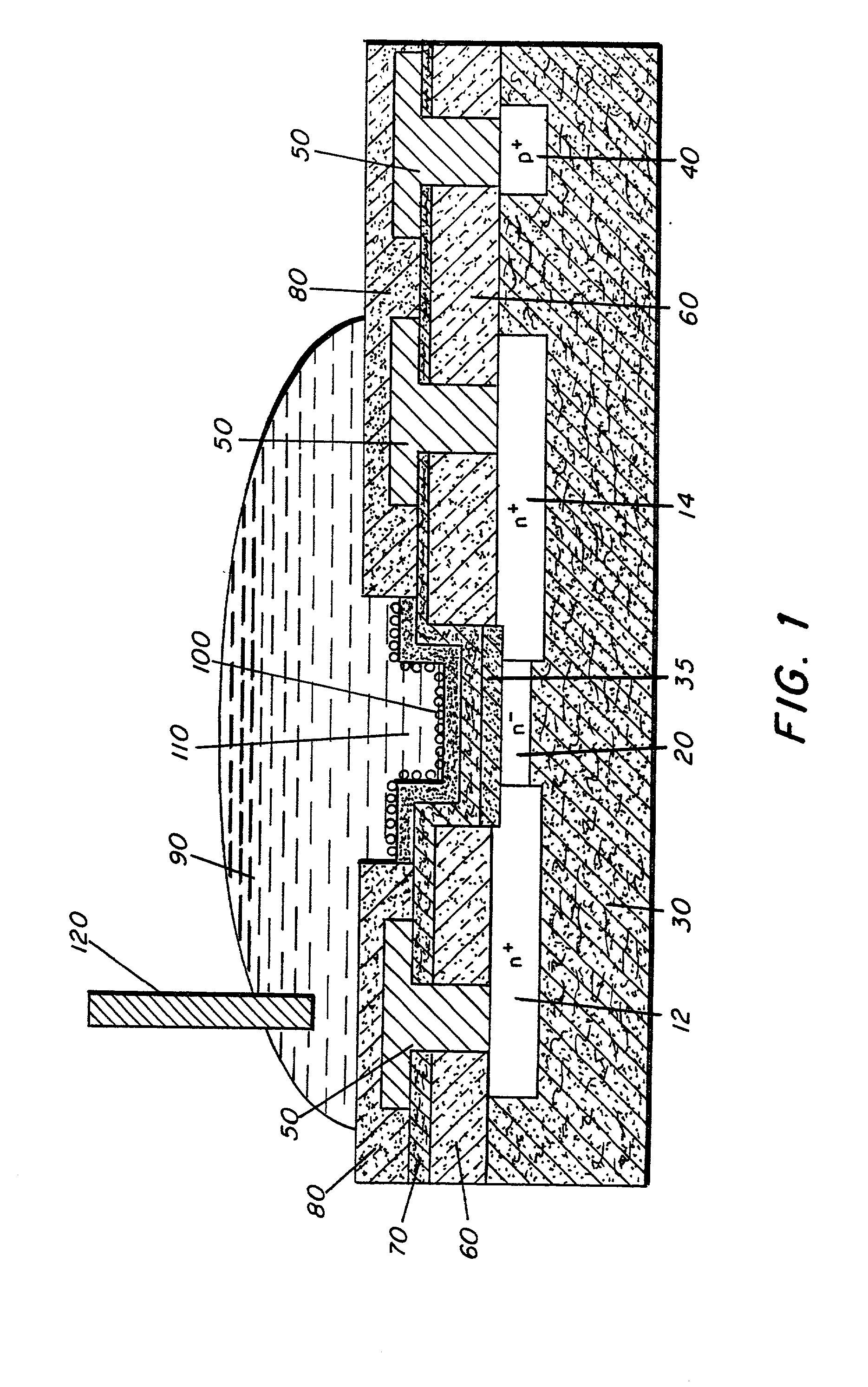
[0034] A source and drain were formed by a P implant in a semiconductor structure at 80 keV to an areal density of 1.times.10.sup.15 cm.sup.-2. The channel region is 32 .mu.m.times.140 .mu.m and P implanted at 60 keV to an areal density of 6.times.10.sup.11 cm.sup.-2. Body contacts were formed by B implantation at 80 keV to 1.times.10.sup.15 cm.sup.-2. A 63 nm thermal oxide layer was followed by a 30 nm LPCVD Si.sub.3N.sub.4 layer. Following a Cr / Au contact metallization, a 600 nm APCVD oxide layer was formed over all. The present example used 36 devices per wafer arranged in 9 groups of 4 on a 6.5 mm pitch. Each device had a separate and independent source and drain contact. Additionally, 14 gated and ungated test structures were included on the wafer for use as reference standards and process and instrumentation diagnostic tools.

[0035] Immobilization procedures have relied on the facile attachment of thiol (-S) ligands to Au evaporated onto the dielectric layer by means of molecul...

example 2

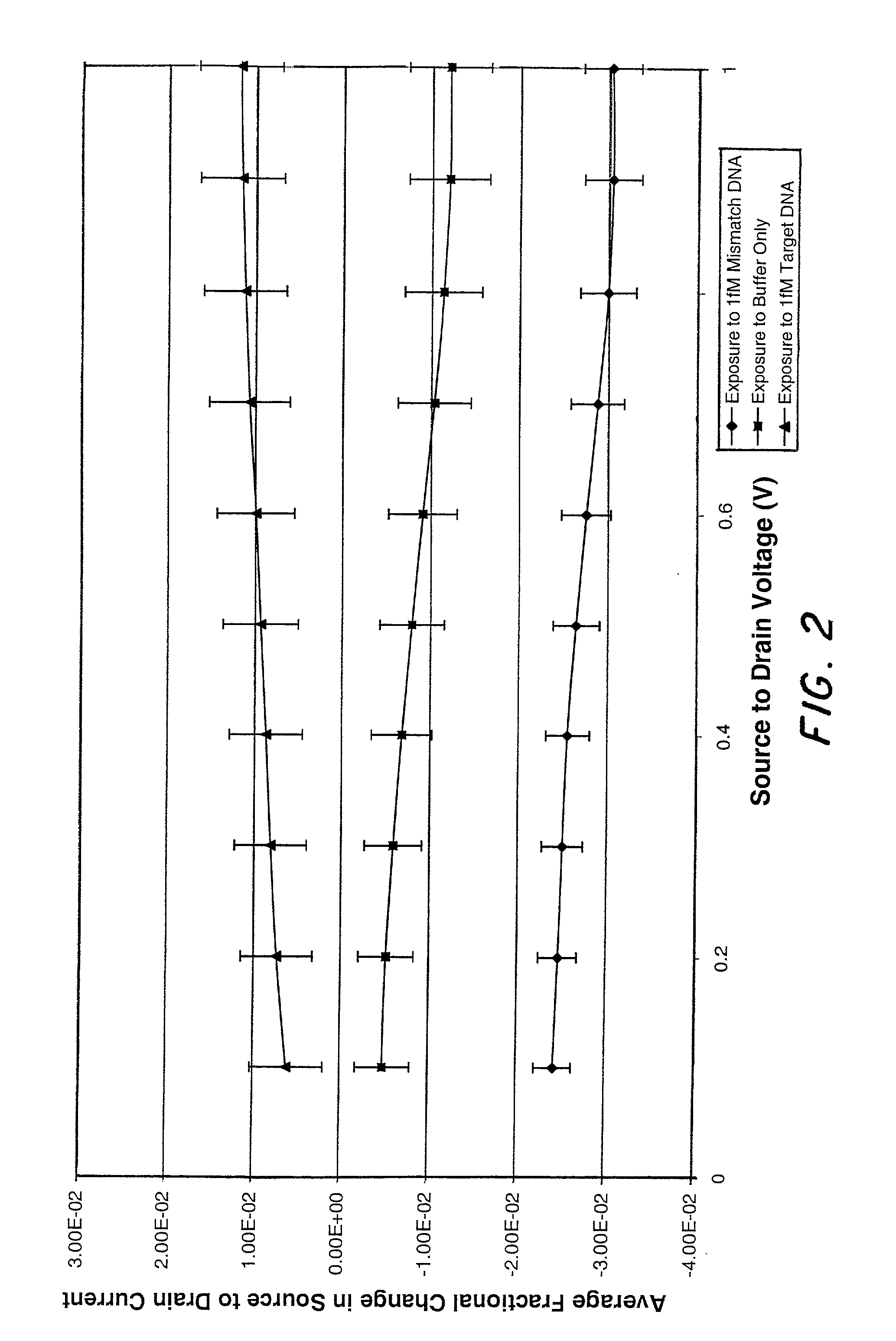
[0038] In contrast to Example 1, the gold modified dielectric layer was in turn modified with thiol terminated single strand DNA. The sensors were exposed to either a solution with 1 fM of single stranded DNA that was complementary to the DNA on the surface, a solution with 1 fM of single stranded DNA that contained a one base pair mismatch to the DNA on the surface, or a blank buffer solution. At this concentration, response to the target DNA was a drop in current of 1.2+ / -0.5%, while the current increased 1.2+ / -0.5% for the devices exposed to the control buffer solution and 3.0+ / -0.3% for those exposed to the mismatch DNA. FIG. 2 shows the typical response of the sensors to the three different solutions plotted as the fractional change in current. The fractional change in source to drain current is (i.sub.SD.sup.before-i.sub.SD.sup.af-ter)i.sub.SD.sup.before.


PUM

PropertyMeasurementUnit
electron mobilityaaaaaaaaaa
dielectric constant εiaaaaaaaaaa

Abstract

Molecular recognition-based electronic sensor, which is gateless, depletion mode field effect transistor consisting of source and drain diffusions, a depletion-mode implant, and insulating layer chemically modified by immobilized molecular receptors that enables miniaturized label-free molecular detection amenable to high-density array formats. The conductivity of the active channel modulates current flow through the active channel when a voltage is applied between the source and drain diffusions. The conductivity of the active channel is determined by the potential of the sample solution in which the device is immersed and the device-solution interfacial capacitance. The conductivity of the active channel modulates current flow through the active channel when a voltage is applied between the source and drain diffusions. The interfacial capacitance is determined by the extent of occupancy of the immobilized receptor molecules by target molecules. Target molecules can be either charged or uncharged. Change in interfacial capacitance upon target molecule binding results in modulation of an externally supplied current through the channel.

Description

[0001] This application claims the benefit of provisional application U.S. Ser. No. 60 / 213,471, filed Jun. 23, 2000, the disclosure of which is incorporated herein by reference.[0002] 1. Field of the Invention[0003] The present invention is a microelectronics-based sensor, specifically, a microelectronics-based transducer for molecular recognition-based sensors for detection or quantification of charged and uncharged target molecules.[0004] 2. Description of the Background Art[0005] Molecular recognition-based sensors are important research tools because of the wide range of target molecules for which receptors can be harvested or synthesized. They have proven indispensable in genomic and pharmaceutical research and development configured in high-density arrays of thousands of individual sensor elements, each element being responsive to a specific target molecule by immobilization of a corresponding molecular receptor. Such arrays enable simultaneous detection of thousands of target...

Claims


Application Information

Patent Timeline
Patent Type & Authority Applications(United States)
IPC IPC(8): G01N27/414G01N33/543
CPCG01N33/54373G01N27/4145H01L2924/0002H01L2924/00
Inventor TENDER, LEONARD M.PECKERAR, MARTINPERKINS, F. KEITHFERTIG, STEPHANIE J.SNOW, ERIC S.
Owner THE UNITED STATES OF AMERICA AS REPRESENTED BY THE SECRETARY OF THE NAVY
Why Eureka
Try Eureka