Ion implantation combined with in situ or ex situ heat treatment for improved field effect transistors

a field effect transistor and heat treatment technology, applied in the field of complementary metal oxide semiconductor (cmos) circuits, can solve the problems of increasing difficulty in maintaining trend, difficult to implant the desired concentration of certain dopant species in the s/d region without amorphizing the entire soi layer, and high defect in s/d recrystallization, so as to avoid or reduce ion implant-induced amorphization and ion implant-induced plastic relaxation

Inactive Publication Date: 2011-06-28
GLOBALFOUNDRIES INC
View PDF8 Cites 103 Cited by
  • Summary
  • Abstract
  • Description
  • Claims
  • Application Information

AI Technical Summary

Benefits of technology

[0015]The present invention teaches the use of ion implantation in combination with in situ or ex situ heat treatments as a method for avoiding or reducing ion implant-induced amorphization and ion implant-induced plastic relaxation.
[0021]In a second embodiment of the invention, ion implantation is combined with ex situ heat treatments in a “divided-dose-anneal-in-between” (DDAB) scheme that avoids the need for tooling capable of performing hot implants. In this embodiment, the desired total dose is divided into smaller sub-doses, each of which is below the threshold for amorphizing the entire thickness of the S / D regions (for the case of UTSOI) or generating significant strain relief (for the case of strained S / D regions). Annealing performed after each implant recrystallizes the amorphized regions by solid phase epitaxy and / or reduces damage accumulation to a negligible level.

Problems solved by technology

This trend is becoming increasingly more difficult to maintain as the devices reach their physical scaling limits.
However, the ion implantation steps used in fabricating the FETs relying on these enhancements present two particular challenges.
It is difficult to implant the desired concentration of certain dopant species in the S / D regions without amorphizing the entire SOI layer.
If there is no crystalline Si left under the amorphized S / D regions to act as a seed or template, the S / D recrystallization will be highly defective (and thus unsuitable for high performance devices).
This is undesirable because doped polycrystalline Si has a much higher resistance than crystalline Si having the same dopant density.
One of the primary challenges in using single-crystal strained regions as a stressor for the channel is to prevent the formation of strain relieving dislocations during strained region growth and subsequent processing.
Certain implantation conditions (particularly those involving heavy ions such as As+) can result in a significant and irreversible reduction in strain after a prescribed thermal treatment step called an “activation anneal.” Since the driving force for strain relaxation increases with strain, SiGe alloys with a high Ge content are particularly susceptible to undesired relaxation.

Method used


Image

  • Ion implantation combined with in situ or ex situ heat treatment for improved field effect transistors
  • Ion implantation combined with in situ or ex situ heat treatment for improved field effect transistors
  • Ion implantation combined with in situ or ex situ heat treatment for improved field effect transistors

Examples


example 1

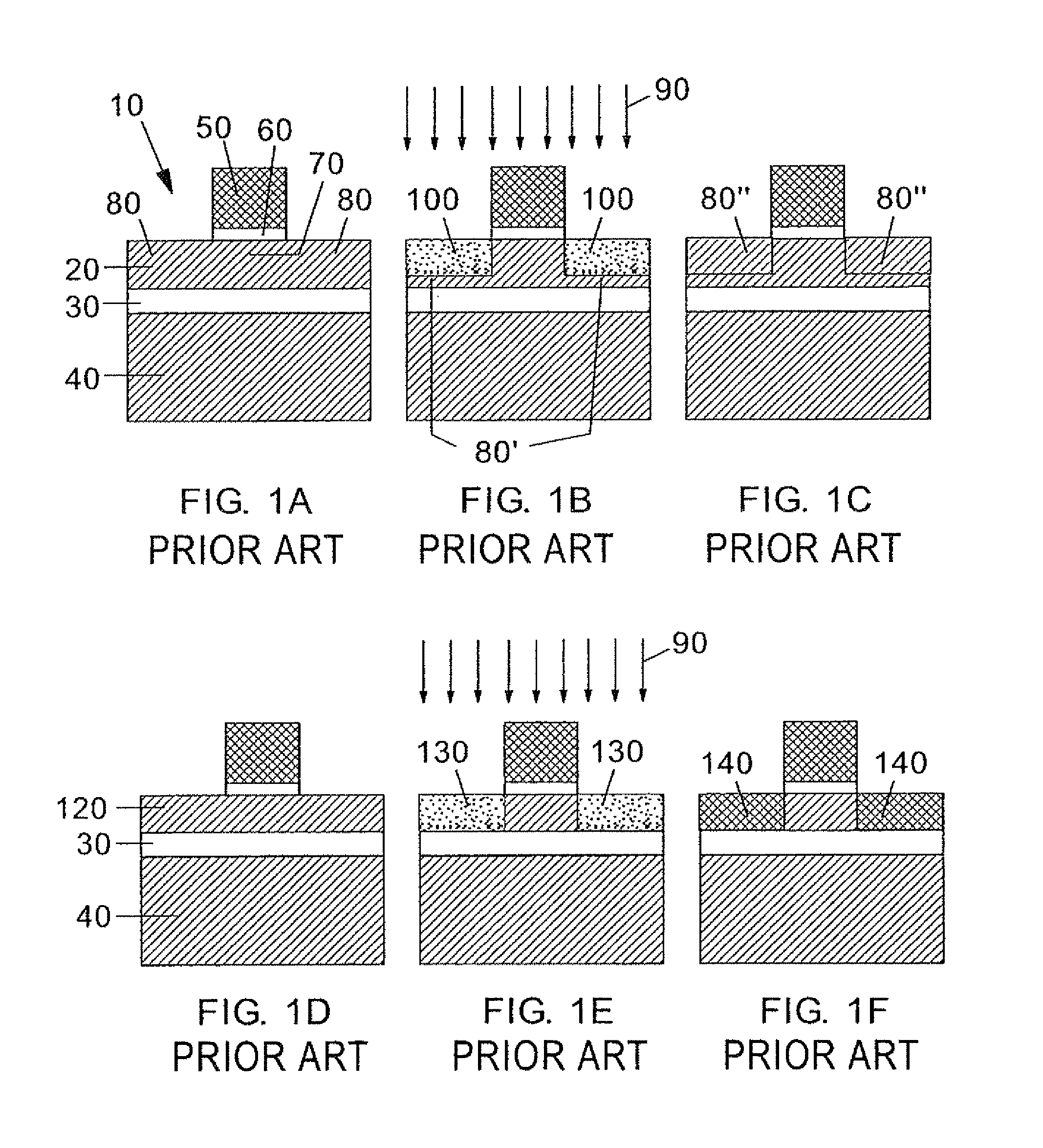
[0085]The example shows that in situ heating during ion implantation can prevent the amorphization of SOI layers that would occur if the same implants were performed at room temperature. SOI layers 28 nm in thickness were implanted at 26, 150, or 300° C. with 3×10¹⁵ / cm2 50 keV As+, an implant that has an average projected range (Rp) of about 340 Å and would ordinarily completely amorphize the SOI layer. The reflectance vs. wavelength data of FIG. 6 indicates that the SOI layer has indeed been amorphized in the 26 and 150° C. samples (curves B and C, respectively), but remains crystalline (with a reflectance curve nearly identical to curve A of the unimplanted control sample) for the 300° C. implant (curve D). The sheet resistance (Rs) measurements of Table I corroborate these results: after annealing in N2 at 900° C. for 1 min, the 26 and 150° C. samples have Rs in the range of 8-11 kohm / square, consistent with a recrystallization of the amorphous SOI layer to polycrystalline Si; in...

example 2

[0088]In the second example, we show how one may use the dependence of amorphization depth on implant dose to calculate an optimum implementation of the DDAB technique in a semiconductor-on-insulator layer disposed on a buried oxide (box). SOI layers 160 nm in thickness were implanted at room temperature with 100 keV As+ (Rp about 71 nm) at doses of 1.25, 2.5, and 5.0×10¹⁵ / cm2 to produce surface amorphous layers having thicknesses of 91, 111, and 117 nm respectively. None of these doses were sufficient to amorphize the entire 160 nm thickness of the SOI layer. However, SOI layers thinner than about 110 nm in thickness would be expected to totally amorphize at doses higher than 2.5×10¹⁵ / cm2, form polycrystalline Si upon activation annealing. Dividing the 2.5×10¹⁵ / cm2 dose into two doses of 1.25×10¹⁵ / cm2 would leave a residual crystalline layer between the 91 nm amorphization depth and the top of the box after each implant. Annealing between the implants allows the crystallinity of th...

example 3

[0089]In the third example, we show how the hot implant and DDAB techniques may be used to preserve the strain in pseudomorphic SiGe layers grown on Si. FIGS. 7-9 show high resolution x-ray diffraction (HRXRD) (004) rocking curves (RCs) of a structure comprised by 40-nm-thick Si0.70Ge0.30 layers epitaxially grown on (100) Si substrate, taken before and after implantation with As+ to a dose below the amorphization threshold dose. In FIGS. 7-9, the ordinate represents the intensity of diffracted x-ray in counts / second and the abscissa represents delta rocking angle omega in unity of seconds of degree, having the scale origin set at the Si substrate diffraction peak. The SiGe peak (at negative angles in FIGS. 7-9) typically comprises a main peak bordered by weaker satellite peaks (thickness fringes or Pendellosung oscillations) whose spacing allows a precise estimate of the SiGe thickness. The intensities of the main peak and the satellite peaks are highest when the SiGe is perfectly o...


PUM


Abstract

This invention teaches methods of combining ion implantation steps with in situ or ex situ heat treatments to avoid and / or minimize implant-induced amorphization (a potential problem for source / drain (S / D) regions in FETs in ultrathin silicon on insulator layers) and implant-induced plastic relaxation of strained S / D regions (a potential problem for strained channel FETs in which the channel strain is provided by embedded S / D regions lattice mismatched with an underlying substrate layer). In a first embodiment, ion implantation is combined with in situ heat treatment by performing the ion implantation at elevated temperature. In a second embodiment, ion implantation is combined with ex situ heat treatments in a “divided-dose-anneal-in-between” (DDAB) scheme that avoids the need for tooling capable of performing hot implants.

Description

RELATED APPLICATIONS[0001]This application is a continuation of U.S. patent application Ser. No. 11 / 417,846, filed May 4, 2006.FIELD OF THE INVENTION[0002]This invention generally relates to complementary metal oxide semiconductor (CMOS) circuits comprising field effect transistors (FETs) fabricated with one or more ion implantation steps. More particularly, it relates to the ways in which these ion implantation steps may be combined with in situ or ex situ heat treatments to avoid and / or minimize implant-induced amorphization (a potential problem for source / drain regions in FETs in ultrathin silicon on insulator layers) and implant-induced plastic relaxation of strained source / drain regions (a potential problem for strained channel FETs in which the channel strain is provided by embedded source / drain regions lattice mismatched with an underlying substrate layer).BACKGROUND OF THE INVENTION[0003]Historically, most performance improvements in semiconductor field-effect transistors (F...

Claims


Application Information

Patent Timeline
Patent Type & Authority Patents(United States)
IPC IPC(8): H01L21/44
CPCH01L21/26513H01L21/324H01L21/84H01L27/1203H01L29/78684H01L29/66628H01L29/66636H01L29/66772H01L29/7848H01L29/78618H01L21/823814H01L29/165Y10S438/909Y10S438/943H01L21/2658
Inventor BEDELL, STEPHEN W.DESOUZA, JOEL P.REN, ZHIBINREZNICEK, ALEXANDERSADANA, DEVANDRA K.SAENGER, KATHERINE L.SHAHIDI, GHAVAM
Owner GLOBALFOUNDRIES INC
Why Eureka
Try Eureka