Method and structure to create multiple device widths in finfet technology in both bulk and soi

Active Publication Date: 2005-07-28
GLOBALFOUNDRIES US INC
View PDF13 Cites 98 Cited by
  • Summary
  • Abstract
  • Description
  • Claims
  • Application Information

AI Technical Summary

Benefits of technology

[0007] The present invention involves putting a spacer on the lower portion of some FinFETs (using a blocking mask to remove/reduce unwanted spacers), and by using several potential doping schemes, making the area protected behind the spacer electrically inactive. When a gate is subsequently patterned o

Problems solved by technology

This limitation in the device design creates difficulty for both porting existing designs into FinFET technology, as well as designing the plethora of circuits that designers have in their toolkit.
The quantization of 1 fin, 2 fins, 3 fins, etc., makes designing

Method used


Image

  • Method and structure to create multiple device widths in finfet technology in both bulk and soi
  • Method and structure to create multiple device widths in finfet technology in both bulk and soi
  • Method and structure to create multiple device widths in finfet technology in both bulk and soi

Examples


Embodiment Construction

[0030] The present invention and the various features and advantageous details thereof are explained more fully with reference to the nonlimiting embodiments that are illustrated in the accompanying drawings and detailed in the following description. It should be noted that the features illustrated in the drawings are not necessarily drawn to scale. Descriptions of well-known components and processing techniques are omitted so as to not unnecessarily obscure the present invention. The examples used herein are intended merely to facilitate an understanding of ways in which the invention may be practiced and to further enable those of skill in the art to practice the invention. Accordingly, the examples should not be construed as limiting the scope of the invention.

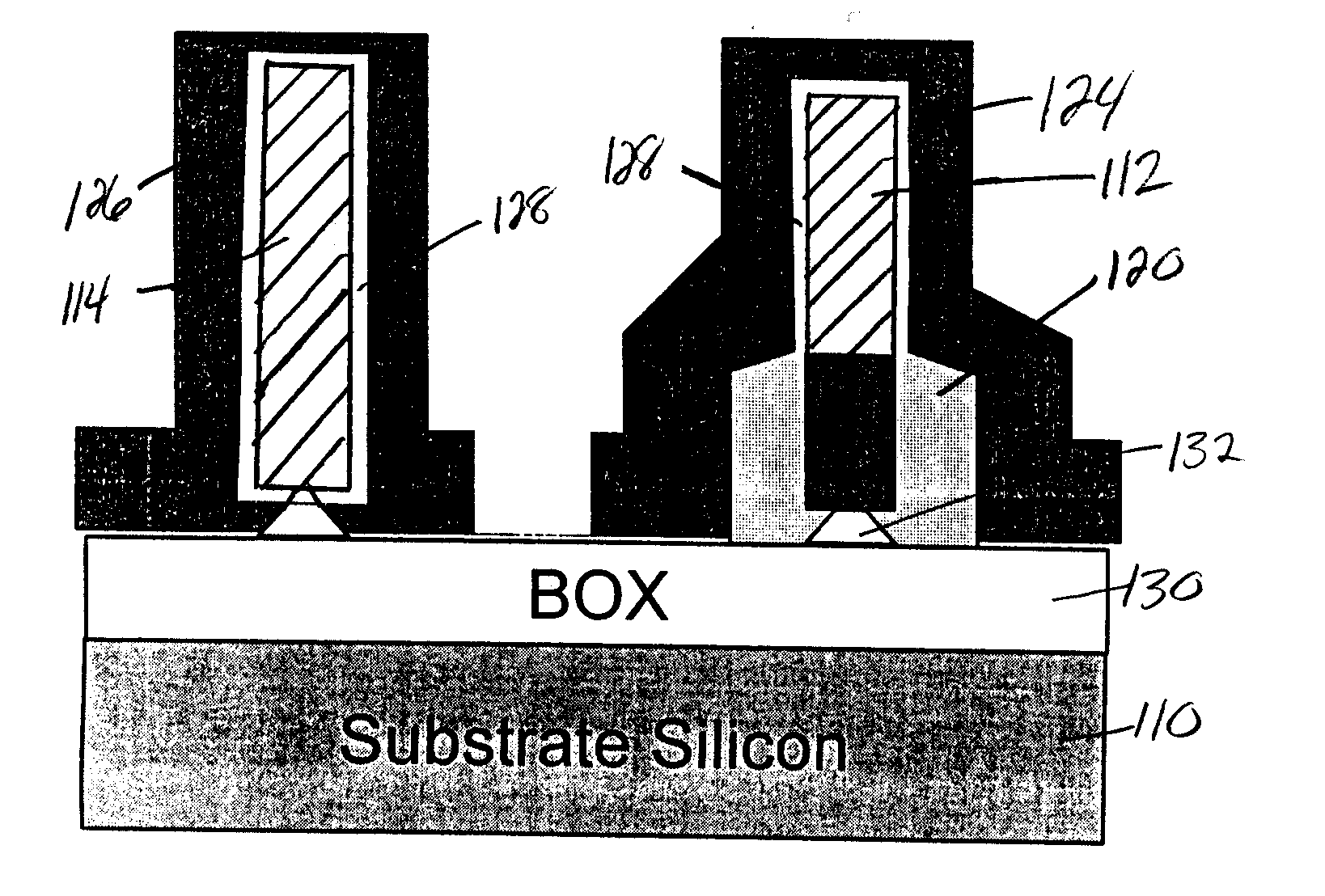
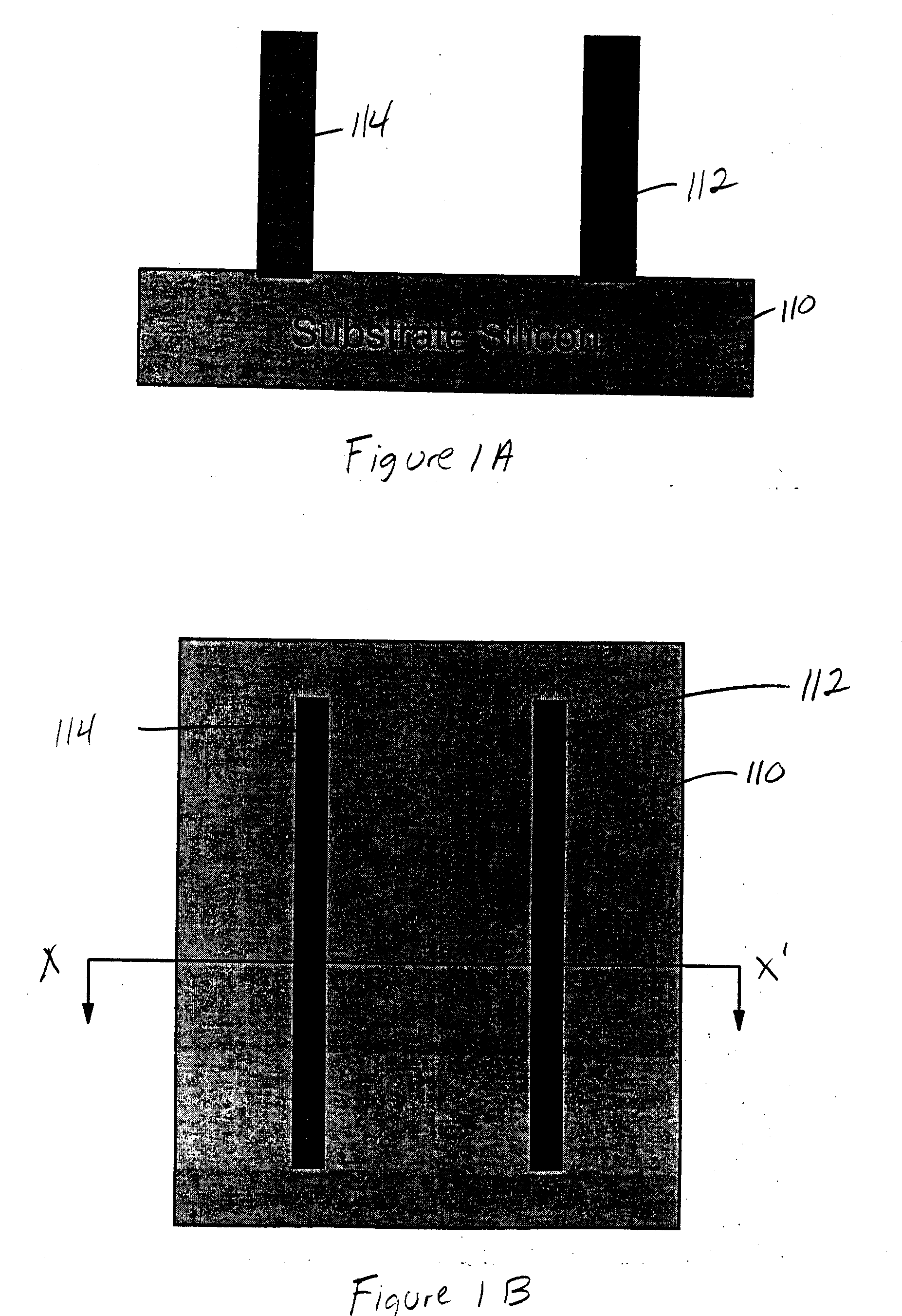
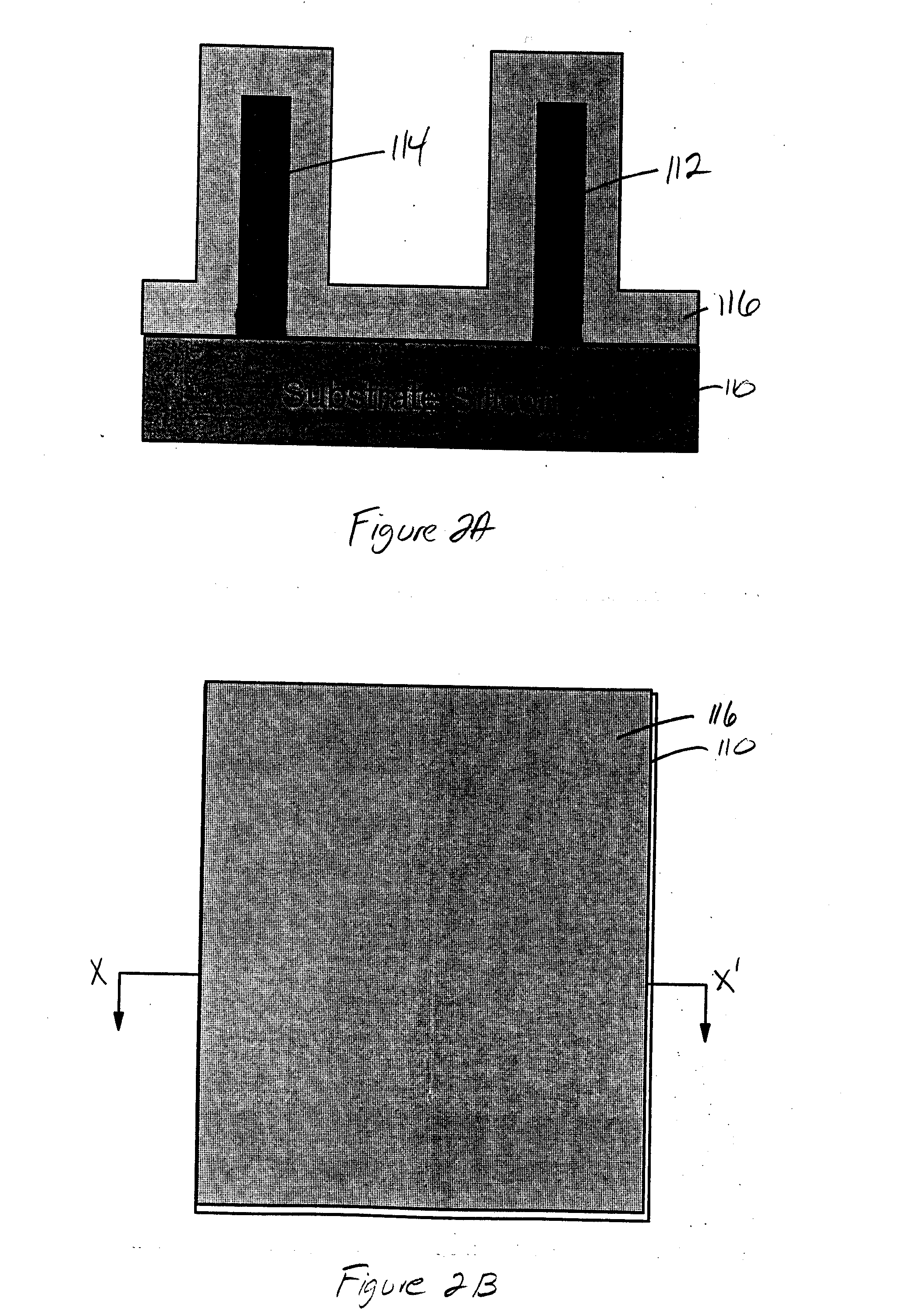
[0031]FIGS. 1A-7B illustrate a bulk silicon substrate embodiment of the invention and FIGS. 8A-14B illustrate a second silicon-on-insulator (SOI) structure. In all the drawings, the “A” Figures represent a cross-sectional ...


PUM


Abstract

Disclosed is a structure and method for producing a fin-type field effect transistor (FinFET) that has a buried oxide layer over a substrate, at least one first fin structure and at least one second fin structure positioned on the buried oxide layer. First spacers are adjacent the first fin structure and second spacers are adjacent the second fin structure. The first spacers cover a larger portion of the first fin structure when compared to the portion of the second fin structure covered by the second spacers. Those fins that have larger spacers will receive a smaller area of semiconductor doping and those fins that have smaller spacers will receive a larger area of semiconductor doping. Therefore, there is a difference in doping between the first fins and the second fins that is caused by the differently sized spacers. The difference in doping between the first fins and the second fins changes an effective width of the second fins when compared to the first fins.

Description

BACKGROUND OF INVENTION [0001] 1. Field of the Invention [0002] The present invention generally relates to fin-type field effect transistor (FinFET) structure and more particularly to an improved structure that includes differently sized spacers adjacent the fins which operate to change the effective width of the fins. [0003] 2. Description of the Related Art [0004] As the end of linear scaling of planar complementary metal oxide semiconductors (CMOS) approaches, alternative device structures are being evaluated. One of the primary candidates is FinFET technology, where a thin fin, or pillar of silicon is created using sub-lithographic techniques, thereby allowing placement of the gate on sides of the Fin, which in the on state, fully depletes the silicon in the fin, making it a high performance device. U.S. Pat. No. 6,413,802 to Hu et al. (hereinafter “Hu”), which is incorporated herein by reference, discloses one example of a FinFET structure. [0005] Conventional CMOS designers ha...

Claims


Application Information

Patent Timeline
IPC IPC(8): H01L21/762H01L21/336H01L21/8234H01L21/84H01L27/08H01L27/088H01L29/786
CPCH01L21/84H01L29/785H01L29/66795H01L29/66803
Inventor ANDERSON, BRENT A.NOWAK, EDWARD J.RANKIN, JED H.
Owner GLOBALFOUNDRIES US INC
Why Eureka
Try Eureka