Monolithic integrated circuit of a field-effect semiconductor device and a diode

a semiconductor device and integrated circuit technology, applied in the direction of diodes, semiconductor devices, electrical devices, etc., can solve the problems of unnecessarily high manufacturing cost, difficult application of parasitic diode technology, and unfavorable use of makeshift measures, etc., to achieve the effect of less cos

Inactive Publication Date: 2007-10-04
SANKEN ELECTRIC CO LTD
View PDF4 Cites 109 Cited by
  • Summary
  • Abstract
  • Description
  • Claims
  • Application Information

AI Technical Summary

Benefits of technology

[0014]Such being the construction of the integrated circuit according to the invention, a current flow is assured from the Schottky electrode to the drain without interruption by a depletion region expanding from the gate means. Thus, monolithically incorporated with the field-effect semiconductor device, the Schottky el

Problems solved by technology

One of the problems with the HEMT of the above familiar design, as well as with the MESFET or other comparable field-effect semiconductor devices, arose when these devices were connected to an inductive or capacitive load.
However, difficulties have been experienced in applying the parasitic diode technology of the IGFET to the HEMT, MESFET and like field-effect semiconductor devices which make use of the two-dimensional electron gas layer as th

Method used


Image

  • Monolithic integrated circuit of a field-effect semiconductor device and a diode
  • Monolithic integrated circuit of a field-effect semiconductor device and a diode
  • Monolithic integrated circuit of a field-effect semiconductor device and a diode

Examples


embodiment

of FIG. 4

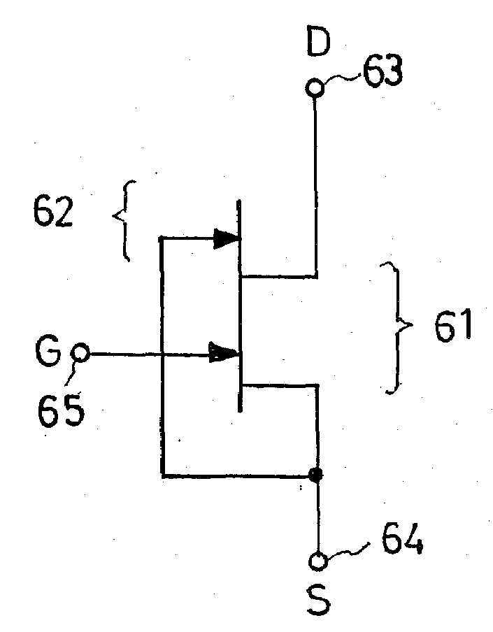
[0051]Difficulties have so far been experienced in making HEMTs, MESFETs and like field-effect semiconductor devices that are “normally off.” The HEMT, for example, of the known standard construction explained at the beginning of this specification was normally on and had to be turned off using a negative power supply for causing the gate to gain a negative potential. Use of such a negative power supply made the associated circuitry unnecessary complex and expensive. The advent of a normally-off HEMT has long been awaited.

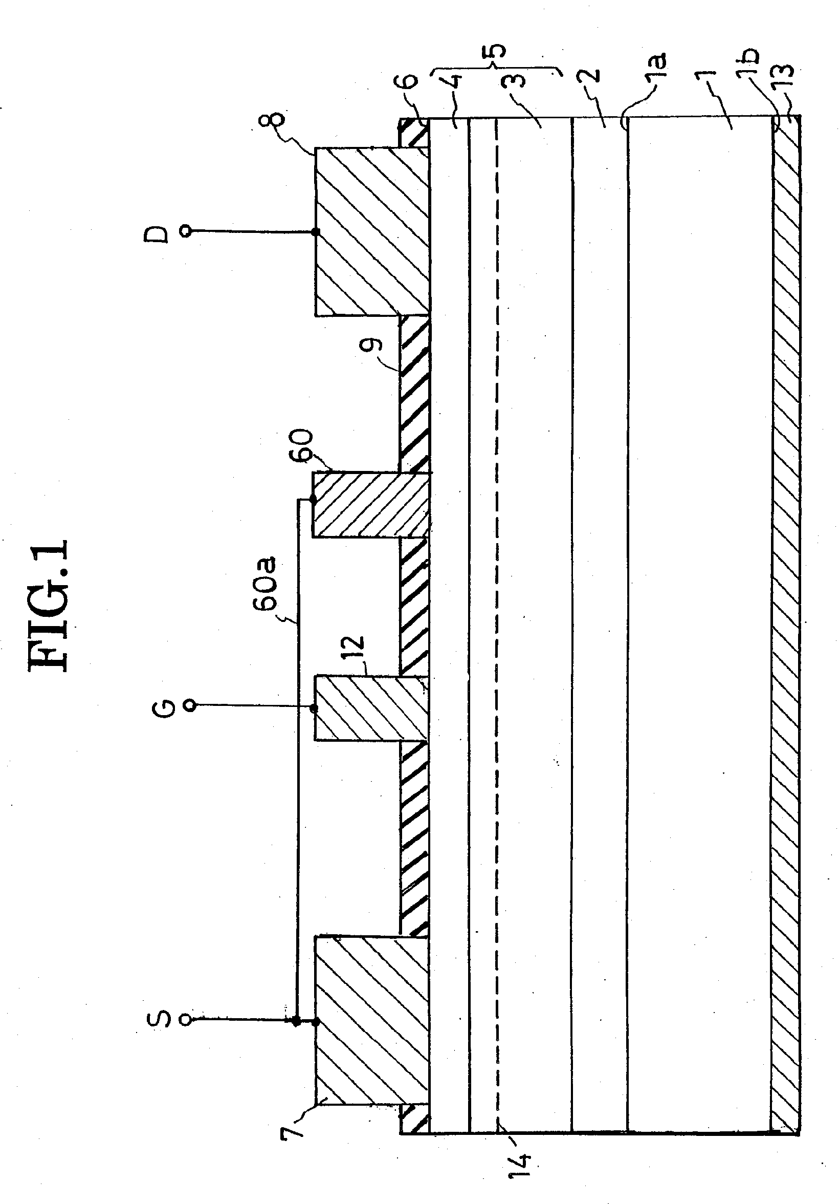
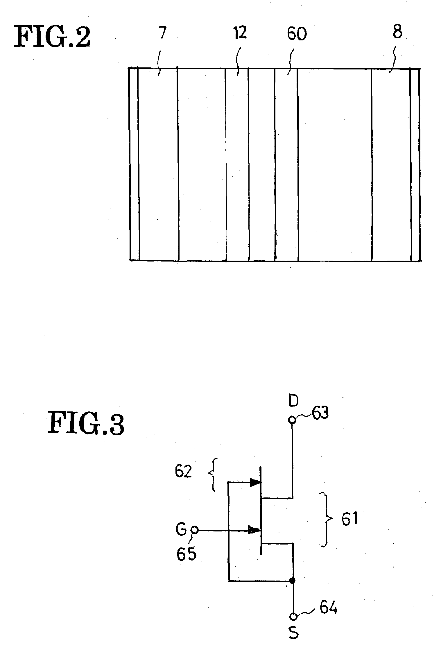
[0052]Drawn in FIG. 4 is a monolithic combination of a normally-off HEMT (or “HEMT-type” device, as will be later explained) and a Schottky diode according to the invention. A comparison of FIGS. 1 and 4 will reveal that this normally-off HEMT / diode combination is similar in construction to the normally-on HEMT / diode combination as far as the substrate 1, buffer region 2, main semiconductor region 5, HEMT electrodes 7, 8 and 13, and diode-creating Schottky...


PUM


Abstract

A field-effect semiconductor device such as a HEMT or MESFET is monolithically integrated with a Schottky diode for feedback, regeneration, or protection purposes. The field-effect semiconductor device includes a main semiconductor region having formed thereon a source, a drain, and a gate between the source and the drain. Also formed on the main semiconductor region, preferably between gate and drain, is a Schottky electrode electrically coupled to the source. The Schottky electrode provides a Schottky diode in combination with the main semiconductor region. A current flow is assured from Schottky electrode to drain without interruption by a depletion region expanding from the gate.

Description

CROSS REFERENCE TO RELATED APPLICATIONS[0001]This application claims priority to Japanese Patent Application No. 2006-098514, filed Mar. 31, 2006, the disclosures of which are incorporated herein by reference in its entirety.BACKGROUND OF THE INVENTION[0002]This invention relates to monolithic integrated circuits and particularly to a monolithic composite integrated circuit of a field-effect semiconductor device and a Schottky diode. The field-effect semiconductor device may take the form of a metal-semiconductor field-effect transistor (MESFET) or high-electron-mobility transistor (HEMT) among others.[0003]The MESFET and HEMT have both been known and used extensively which are made from semiconducting nitrides. Japanese Unexamined Patent Publication No. 2005-158889 is hereby cited as dealing with these kinds of semiconductor devices.[0004]Let us more closely study the typical prior art construction of the HEMT for example. It comprises an electron transit layer of undoped GaN overl...

Claims


Application Information

Patent Timeline
IPC IPC(8): H01L29/94H01L27/095
CPCH01L27/0605H01L27/0255H01L27/0629H01L27/0727H01L29/66431H01L29/778
Inventor SUZUKI, MIOIWABUCHI, AKIO
Owner SANKEN ELECTRIC CO LTD
Why Eureka
Try Eureka