POGO pin and test socket including the same

a technology of test socket and pogo pin, which is applied in the direction of semiconductor/solid-state device testing/measurement, measurement devices, instruments, etc., can solve the problems of severe shortened life of pogo pin b>30/b>, difficult use, and incurred problems

Inactive Publication Date: 2006-07-06
SAMSUNG ELECTRONICS CO LTD
View PDF7 Cites 18 Cited by
  • Summary
  • Abstract
  • Description
  • Claims
  • Application Information

AI Technical Summary

Benefits of technology

[0022] The stepped portion is adapted to limit the movement of the metal plunger so that it is not pushed out through the back side of the receiving aperature.

Problems solved by technology

One drawback of the convention POGO pin 30 as shown in FIG. 1 is problems incurred when shorter contacting test pins are required.
If the conventional POGO pin 30 is manufactured having a length below 3 mm, the life span of the POGO pin 30 is severely shortened, making it difficult to use.
This is because RF signals are greatly affected by parasitic inductance and capacitance.
Accordingly, the conventional POGO pin 30 is not suitable for testing RF products.
However, the rubber contact pin 50 used in the prior art has the disadvantage of a short life span due to use of the rubber material.

Method used


Image

  • POGO pin and test socket including the same
  • POGO pin and test socket including the same
  • POGO pin and test socket including the same

Examples


Embodiment Construction

[0029] The present invention will now be described more fully with reference to the accompanying drawings, in which exemplary embodiments of the invention are shown. The invention may, however, be embodied in many different forms and should not be construed as being limited to the embodiments set forth herein; rather, these embodiments are provided so that this disclosure will be thorough and complete, and will fully convey the concept of the invention to those skilled in the art.

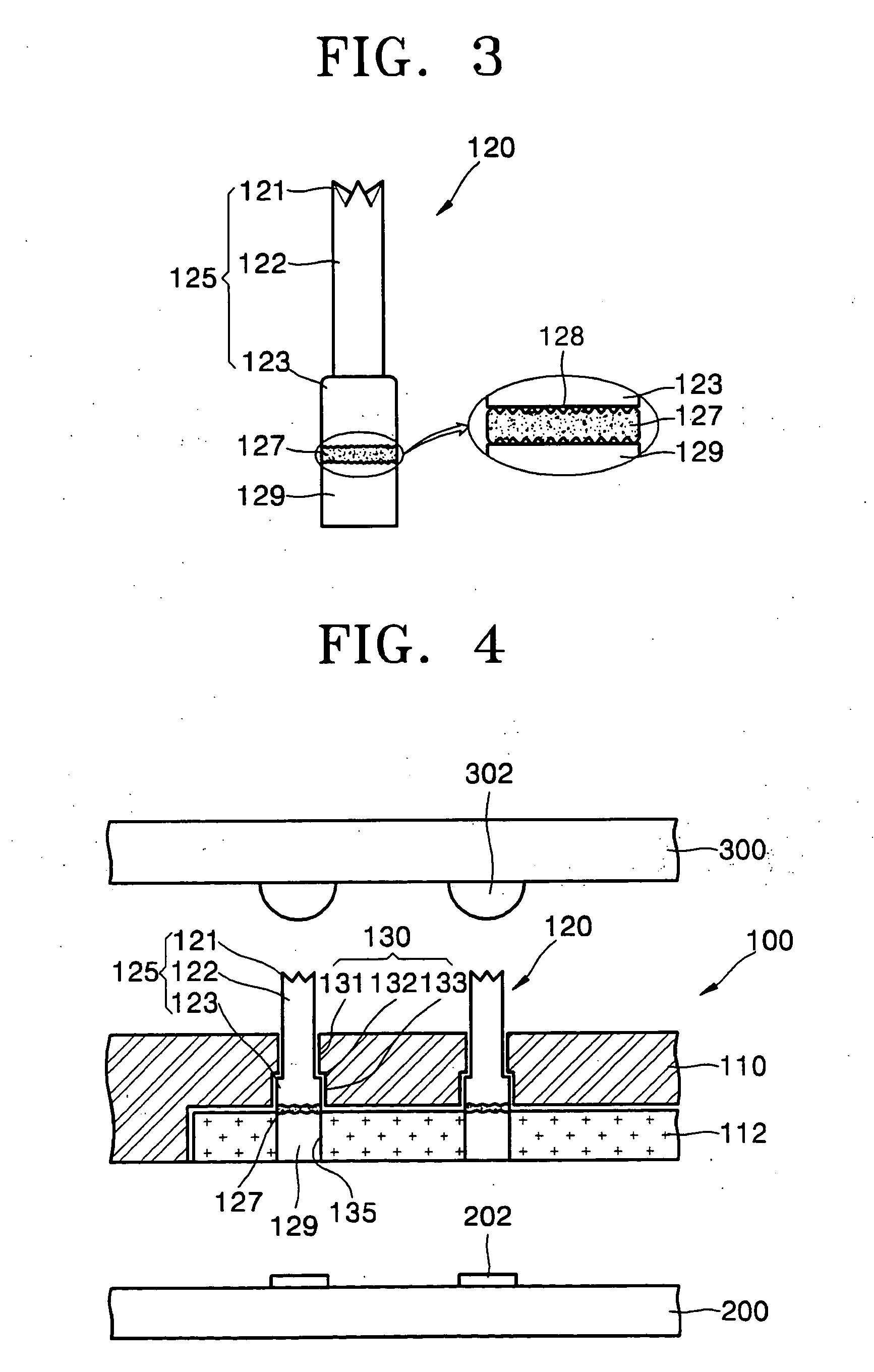
[0030] The present invention relates to a POGO pin 120 of a test socket (see 100 of FIG. 4). A method for mounting the POGO pin 120 in the test socket 100 can be variously modified without being limited to the following embodiment.

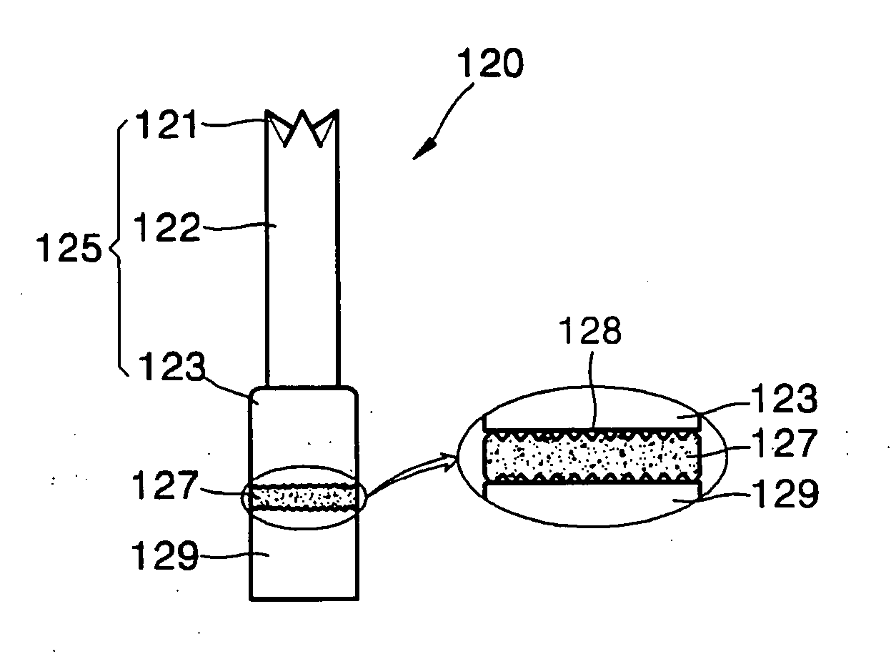
[0031]FIG. 3 is a perspective view of a POGO pin according to the present invention. Referring to FIG. 3, the POGO pin 120 includes a metal plunger 125 electrically contacting a semiconductor package, and a rubber contact pin 129 coupled to the metal plunger 125 and electrically...


PUM


Abstract

A POGO pin that can measure low frequency products as well as RF products and also have a long life span, and a test socket including the POGO pin are provided. The POGO pin includes a metal plunger formed of a conductive metal so as to electrically contact the semiconductor package, and a rubber contact pin connected with the metal plunger and formed of a conductive rubber so as to electrically contact the test board.

Description

CROSS-REFERENCE TO RELATED PATENT APPLICATION [0001] This application claims the benefit of Korean Patent Application No. 10-2005-0000811, filed on Jan. 5, 2005, in the Korean Intellectual Property Office, the disclosure of which is incorporated herein in its entirety by reference. BACKGROUND OF THE INVENTION [0002] 1. Field of the Invention [0003] The present invention relates to a semiconductor package reliability tester, and more particularly, to a POGO pin for testing the electrical characteristics of a semiconductor package and a test socket including the POGO pin. [0004] 2. Description of the Related Art [0005] Semiconductor devices that have undergone patterning processes are subjected to an electrical die sorting (EDS) test using a probe unit. After the EDS test, the semiconductor devices are packaged in semiconductor packages via a series of packaging processes. Then, the semiconductor packages are electrically tested using a test socket before they are shipped as products ...

Claims


Application Information

Patent Timeline
Patent Type & Authority Applications(United States)
IPC IPC(8): G01R31/02
CPCG01R1/0466G01R1/06722G01R1/0483H01L22/00
Inventor JEONG, HYECK-JINPARK, JUNG-HYUNKIM, HEUI-SEOGJEON, JONG-KEUNYOON, SEOK-YOUNG
Owner SAMSUNG ELECTRONICS CO LTD
Why Eureka
Try Eureka