Electrical contact method and structure for deflection devices formed in an array configuration

a technology of array configuration and electrical contact, applied in the field of manufacturing objects, can solve the problems of adversely affecting the response time of individual elements of the mems array, techniques that have limitations, etc., and achieve the effects of reducing propagation delays, improving integrated structure, and being convenient to us

Active Publication Date: 2006-07-13
MIRADIA INC
View PDF61 Cites 27 Cited by
  • Summary
  • Abstract
  • Description
  • Claims
  • Application Information

AI Technical Summary

Benefits of technology

[0008] Many benefits are achieved by way of the present invention over conventional techniques. For example, the present technique provides an easy to use process that relies upon conventional technology. In some embodiments, the method provides reduced propagation delays for bias signals. Additionally, the method provides a process that is compatible with conventional process technology without substantial modifications to conventional equipment and processes. Preferably, the invention provides for an improved integrated structure including integrated circuits and mirror structures for display applications. Depending upon the embodiment, one or more of these benefits may be achieved. These and other benefits will be described in more throughout the present specification and more particularly below.

Problems solved by technology

Unfortunately, these techniques also have limitations.
For example, an extended current path may result in propagation delays that can adversely impact the response time of individual elements of the MEMS array.

Method used


Image

  • Electrical contact method and structure for deflection devices formed in an array configuration
  • Electrical contact method and structure for deflection devices formed in an array configuration
  • Electrical contact method and structure for deflection devices formed in an array configuration

Examples


Embodiment Construction

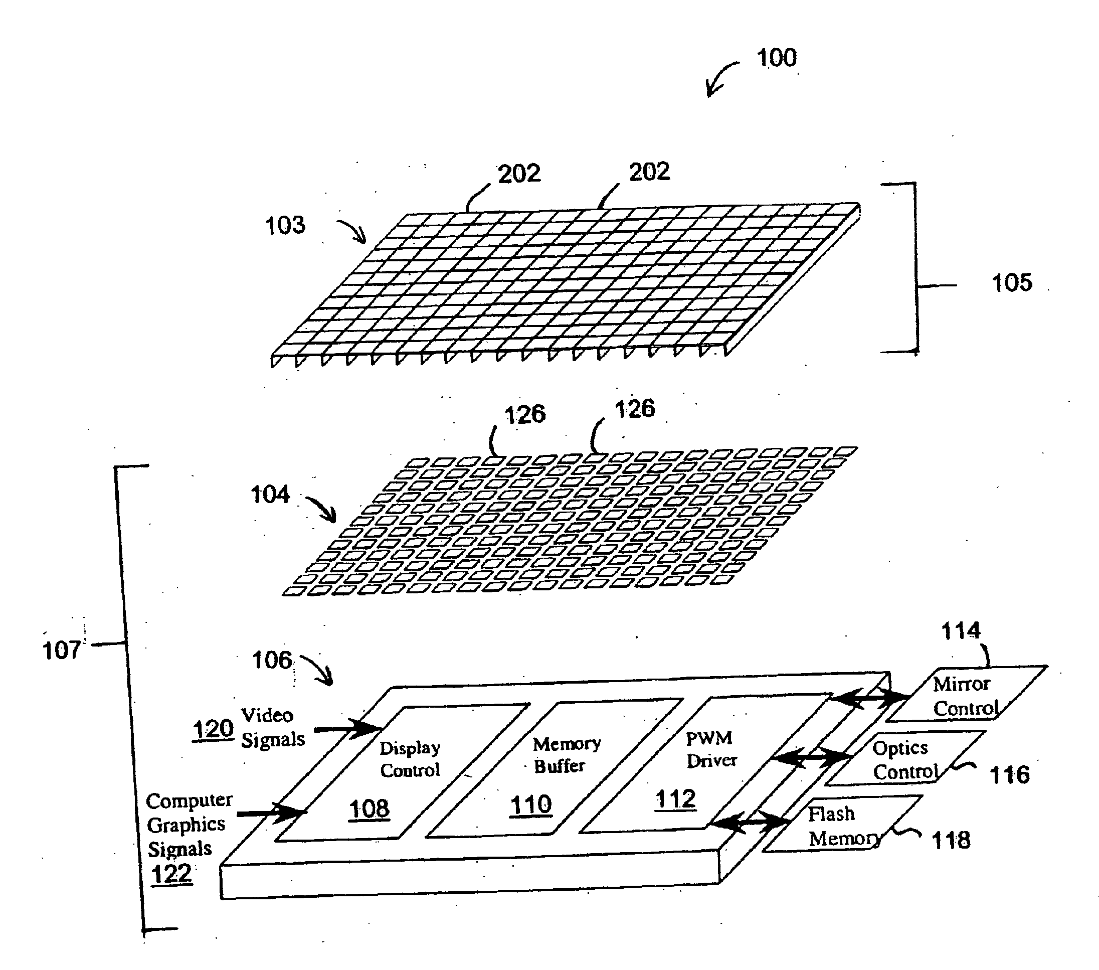
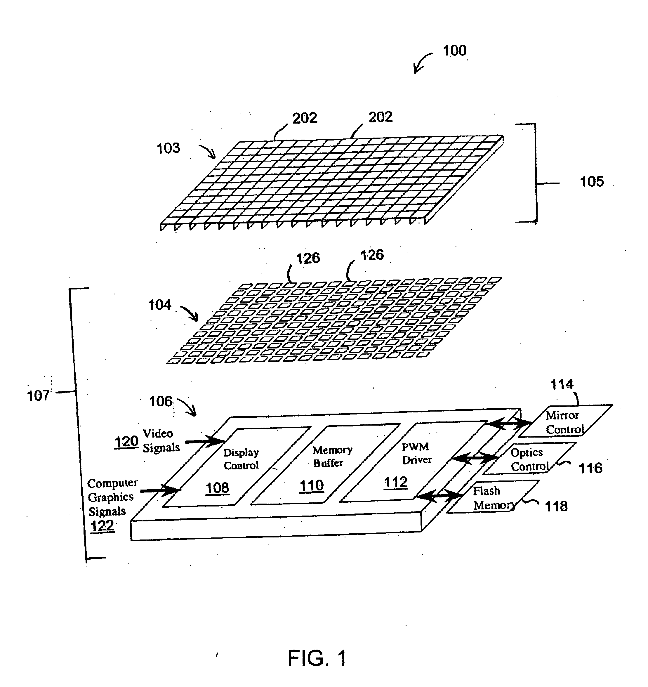
[0016] According to the present invention, techniques for manufacturing objects are provided. More particularly, the invention includes a method and structure for fabricating electrical connections for spatial light modulators. Merely by way of example, the invention has been applied to the formation of an electrical connector running from a bias grid on a substrate to a reflective surface deposited on a mirror structure. The method and structure can be applied to spatial light modulators as well as other devices, for example, micro-electromechanical sensors, detectors, and displays.

[0017]FIG. 1 is a diagram that illustrates the general architecture of a spatial light modulator (SLM) 100 according to one embodiment of the invention. The illustrated embodiment has three layers. The first layer is a mirror array 103 that has a plurality of deflectable micro-mirrors 202. In one preferred embodiment, the micro-mirror array 103 is fabricated from a first substrate 105 that is a single m...


PUM


Abstract

A method of fabricating an electrical connection for a spatial light modulator includes providing a first substrate including a plurality of bias electrodes and a plurality of dielectric bond pads. The method also includes providing a second substrate of a predetermined thickness, the second substrate including a plurality of recessed regions within the predetermined thickness and arranged in a spatial manner as a second array, each of the recessed regions being bordered by a standoff region, and joining the dielectric bond pads of the first substrate to the standoff region of the second substrate. The method further includes forming mirror structures from a first portion of the second substrate, exposing a portion of the upper surface of the plurality of bias electrodes, and depositing a conductive layer on the mirror structures and the exposed portion of the upper surface of the plurality of bias electrodes.

Description

BACKGROUND OF THE INVENTION [0001] This present invention relates generally to manufacturing objects. More particularly, the invention relates to a method and structure for fabricating electrical connections for spatial light modulators. Merely by way of example, the invention has been applied to the formation of an electrical connector running from a bias grid on a substrate to a reflective surface deposited on a mirror structure. The method and structure can be applied to spatial light modulators as well as other devices, for example, micro-electromechanical sensors, detectors, and displays. [0002] Micro-electromechanical systems (MEMS) are used in a number of application areas. For example, MEMS have been used in micro-mirror arrays, sensors, and actuators. In some of these applications, a suspended member is supported by a flexible hinge attached to a stationary portion of the mirco-mirror array. Flexibly attached to the hinge, the suspended member is attracted to an electrode u...

Claims


Application Information

Patent Timeline
Patent Type & Authority Applications(United States)
IPC IPC(8): G02B26/00
CPCG02B26/0816
Inventor YANG, XIAO
Owner MIRADIA INC
Why Eureka
Try Eureka