Optical semiconductor device

Active Publication Date: 2006-07-27
ROHM CO LTD
View PDF4 Cites 39 Cited by
  • Summary
  • Abstract
  • Description
  • Claims
  • Application Information

AI Technical Summary

Benefits of technology

[0007] The present invention has been conceived under the above-described circumstances. It is therefore an object of the present invention to

Problems solved by technology

However, in such a case, following problem may be caused.
As it is technically difficult to obtain a 100% opti

Method used


Image

  • Optical semiconductor device
  • Optical semiconductor device
  • Optical semiconductor device

Examples


first embodiment

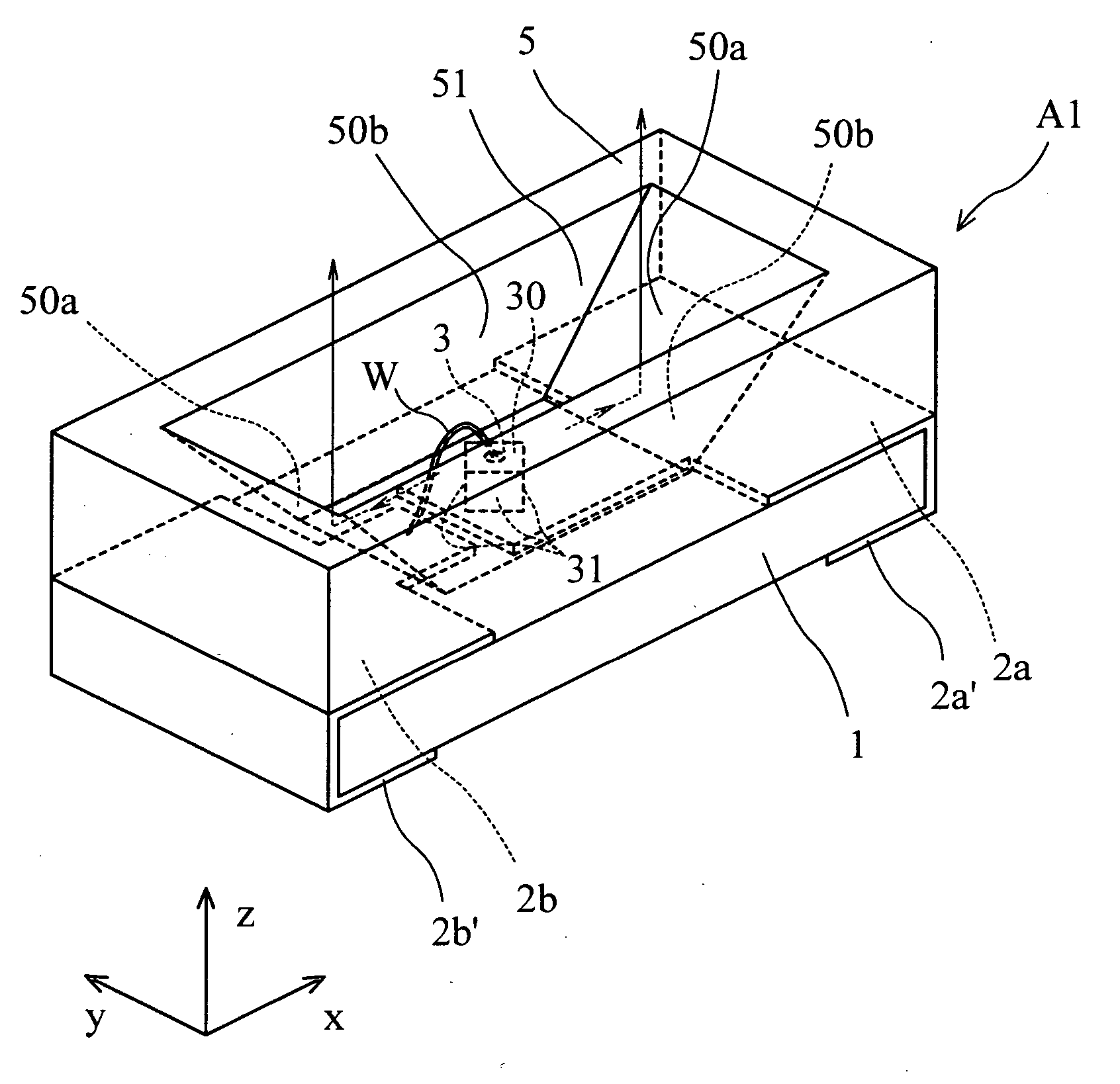
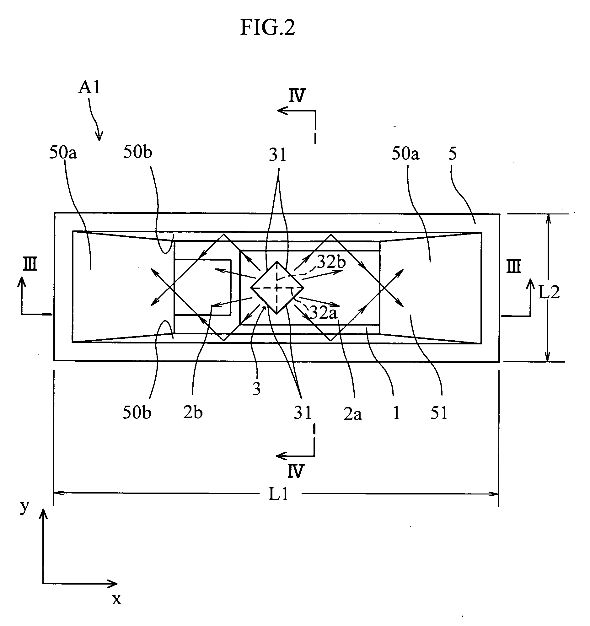
[0033]FIGS. 1-4 illustrate an optical semiconductor device A1 according to the present invention. In FIG. 1, a coordinate system is set along the directions x, y, and z, relative to the optical semiconductor device A1. Each of the three directions is perpendicular to the other two directions, and the direction z is the vertical direction of the device (the arrangement is the same for other embodiments). FIG. 2 shows the optical semiconductor device A1 viewed in the direction z (or viewed parallel to the direction z) from a viewpoint above the optical semiconductor device A1. FIG. 3 is a sectional view taken along lines III-III in FIG. 2, and FIG. 4 is a sectional view taken along lines IV-IV in FIG. 2.

[0034] The optical semiconductor device A1 includes a rectangular insulating base plate 1, an LED chip 3, a reflector 5, and a light-permeable member 6. The light-permeable member 6 is not shown in FIGS. 1 and 2.

[0035] The base plate 1 is made of a glass epoxy resin, for example. The ...

second embodiment

[0046]FIG. 5 illustrates an optical semiconductor device A2 according to the present invention. The optical semiconductor device A2 includes three LED chips 3 accommodated in the reflector 5. These LED chips 3 are aligned and spaced from each other in the direction x, and every one of them is arranged the same as the LED chip shown in FIG. 2 (specifically, the side surfaces 31 are inclined at 45° relative to the x axis and the y axis).

[0047] This structure can also make the light, that is emitted from the side surfaces 31 of the LED chips 3 and travels toward the second reflecting surface 50b, to be guided to the first reflecting surface 50a, and to be upwardly reflected at the first reflecting surfaced 50a to above the optical semiconductor device A2. The LED chips 3 may emit light of a same color, or of different colors (R, G, B). The LED chips 3 may also drive at the same time, or only one or two selected chips may drive at a time.

third embodiment

[0048]FIG. 6A illustrates an optical semiconductor device A3 of the present invention. In the optical semiconductor device A3, each of the side surfaces 31 of the LED chip 3 is arranged parallel to any one of the directions x and y (and parallel to the direction z). Each of the second reflecting surfaces 50b of the reflector 5 is formed with a projection 53 protruding toward the LED chip 3. The projection 53 faces one side surface (one of the two side surfaces 31a spaced from each other in the direction y) of the LED chip 3. The projection 53 is triangular in section and includes a pair of walls (reflecting surfaces) 53a for light reflection. Each of the reflecting surfaces 53a is parallel to the direction z, while non-parallel to both of the directions x and y. The reflecting surfaces 53a are inclined relative to the direction x at 45°, for example. Thus, the reflecting surfaces 53a are non-parallel to the side surfaces 31a that are parallel to the directions x and y.

[0049] Due to...


PUM


Abstract

An optical semiconductor device (A1) comprises a light reflector (5) and an optical semiconductor chip (3). The reflector (5) includes two first reflecting surfaces (50a) spaced from each other in direction x, and two second reflecting surfaces (50b) spaced from each other in direction y. The chip (3) includes a rectangular upper surface and a rectangular lower surface spaced from each other in direction z perpendicular to both of the directions x and y. The chip (3) further includes at least one light-emitting surface (31) extending between the upper and the lower surfaces. The light-emitting surface (31) faces a corresponding one of the second reflecting surfaces (50b). The light-emitting surface (31) is non-parallel to the corresponding second reflecting surfaces (50b) as viewed in parallel to the direction z.

Description

TECHNICAL FIELD [0001] The present invention relates to an optical semiconductor device comprising an optical semiconductor chip such as a LED chip. The present invention especially relates to an optical semiconductor device comprising a reflector for improving illumination efficiency. BACKGROUND ART [0002] An example of a conventional optical semiconductor device is disclosed in a following patent document 1. FIGS. 7-9 illustrate the structure of this optical semiconductor device. The illustrated optical semiconductor device B includes a base plate 101, an LED chip 103 mounted on the base plate, and a reflector 105 surrounding the LED chip 3. As shown in FIG. 8, the reflector 105 is a rectangular frame. As shown in FIG. 9, a space defined by the reflector 105 is filled with a transparent protective resin 106 for covering the LED chip 103 and a wire 104 connected to the chip (the protective resin 106 is not shown in FIGS. 7 and 8). The reflector 105 includes two pairs of inner surfa...

Claims


Application Information

Patent Timeline
IPC IPC(8): H01L33/00H01L29/24H01L25/075H01L33/56H01L33/60
CPCH01L25/0753H01L33/60H01L2224/48091H01L2224/48465H01L2924/00014H01L2924/00
Inventor ISOKAWA, SHINJI
Owner ROHM CO LTD
Why Eureka
Try Eureka