Semiconductor sensor
- Summary
- Abstract
- Description
- Claims
- Application Information
AI Technical Summary
Benefits of technology
Problems solved by technology
Method used
Image

Examples
first embodiment
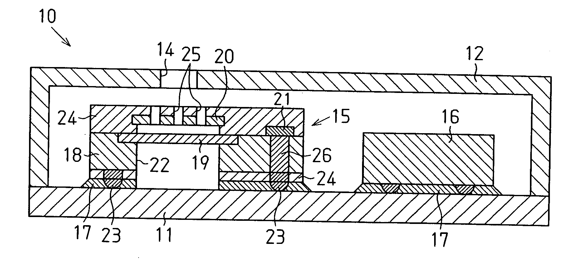
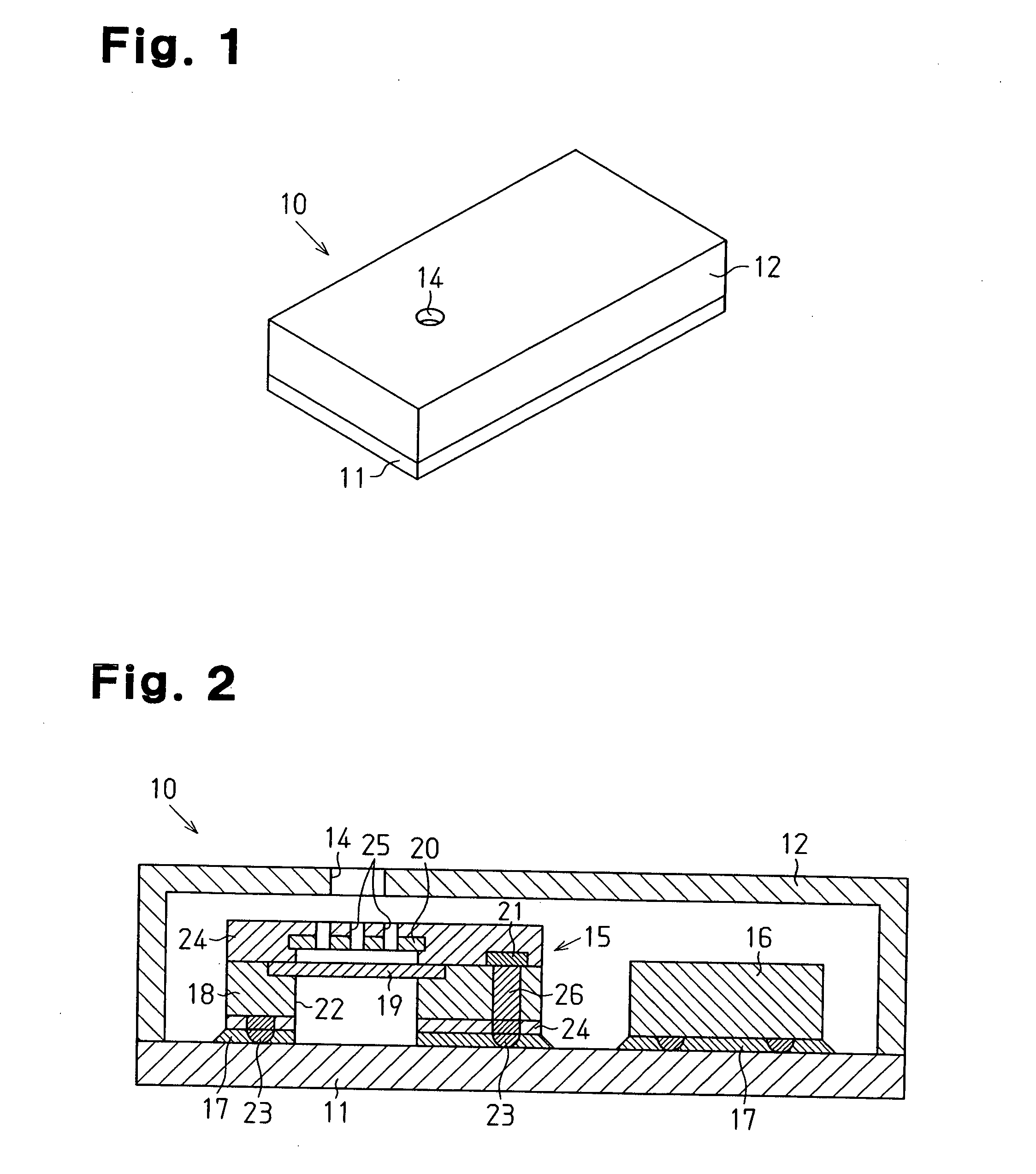
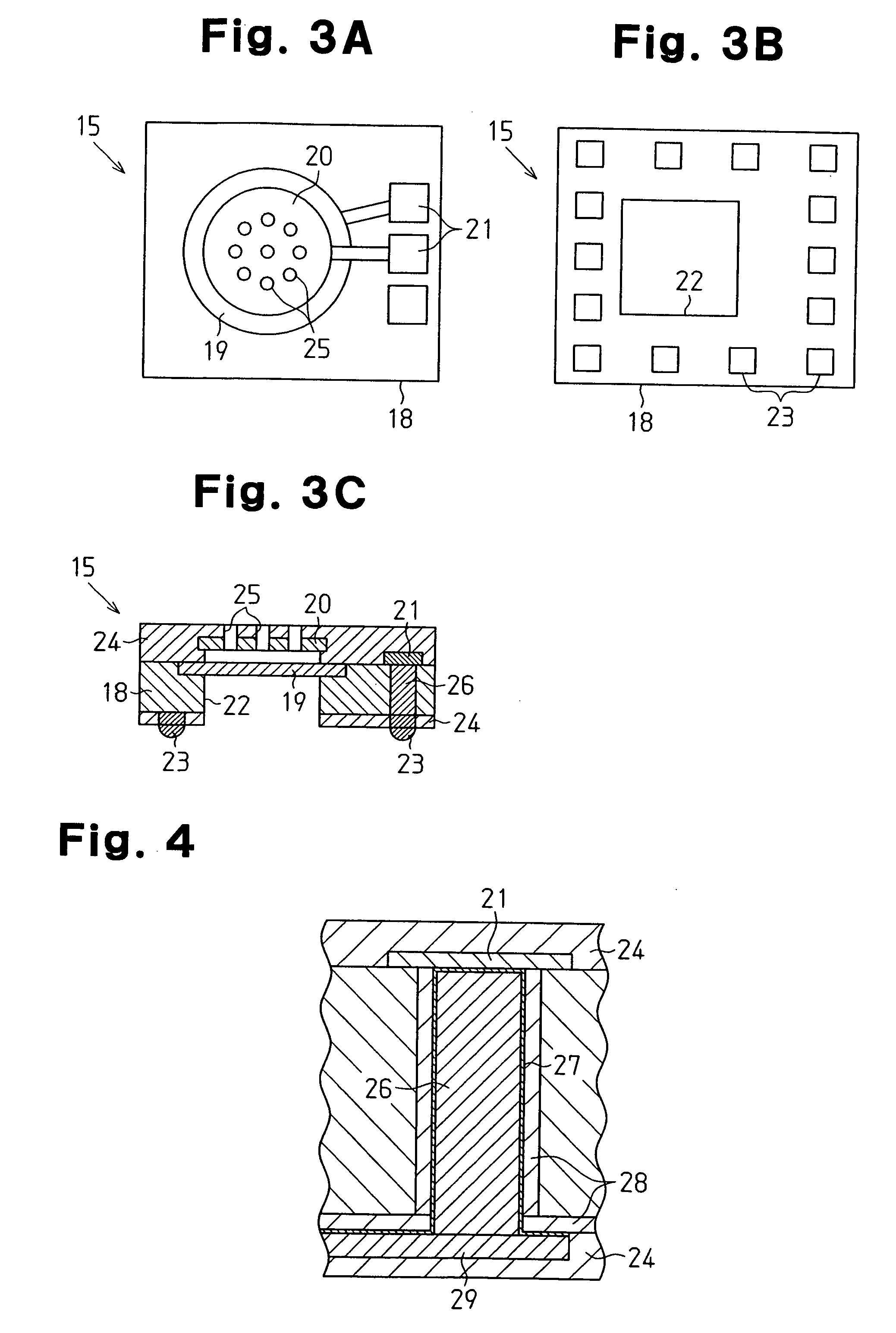
[0040] The semiconductor sensor of the first embodiment has the advantages described below.
[0041] The through electrode 26 directly connects the MEMS configuration formed on the upper surface of the semiconductor substrate 18 to the wiring of the printed wiring board 11. Thus, there is no need for wire bonding to connect the MEMS configuration and the printed wiring board 11. This obtains a semiconductor sensor that increases manufacturing productivity without causing problems, such as enlargement of the packaging area, manufacturing defects resulting from ultrasonic vibrations, and increase in manufacturing costs.
[0042] A semiconductor sensor according to a second embodiment of the present invention will now be described with reference to FIGS. 5 and 6. To avoid redundancy, like or same reference numerals are given to those components that are the same as the corresponding components of the first embodiment. Such components will not be described.
second embodiment
[0043] As shown in FIG. 6, a package module 33 of the second embodiment includes an integrated chip 30, which integrates both functions of the microphone chip 15 and the IC chip 16 shown in FIG. 2. The integrated chip 30 serves as a sound detection unit, that is, a semiconductor sensor. The integrated chip 30 enables the package module 33 to be miniaturized and reduces the manufacturing cost.
[0044] As shown in FIG. 5A, the integrated chip 30 includes a microphone control integrated circuit 32 formed on the upper surface of the semiconductor substrate 31. The integrated circuit 32 is directly wire-connected to the diaphragm electrode 19 and the fixed electrode 20. The integrated circuit 32 is also wire-connected to a plurality of electrode pads 21.
[0045] As shown in FIG. 5C, the semiconductor substrate 31 includes through electrodes 26 formed at positions corresponding to the electrode pads 21, which are wire-connected to the integrated circuit 32. Each through electrode 26 extends ...
third embodiment
[0048] A semiconductor sensor according to the present invention will now be described with reference to FIG. 7 to FIG. 8.
[0049] An integrated chip 40, which functions as a sound detection unit or a semiconductor sensor, includes a diaphragm electrode 19 formed on the upper surface of a semiconductor substrate 41 and a microphone control integrated circuit 42 formed on the lower surface of the semiconductor substrate 41. The through electrodes 26 facilitate the electrical connection between the MEMS configuration (19, 20) and the integrated circuit 42 formed on opposite surfaces of the semiconductor substrate 41.
[0050] As shown in FIG. 7A, the diaphragm electrode 19, the fixed electrode 20, and the electrode pads 21, which are connected to the diaphragm electrode 19 and the fixed electrode 20, are formed on the upper surface of the semiconductor substrate 41. As shown in FIG. 7B, the integrated circuit 42 is formed on the lower surface of the semiconductor substrate 41. As shown in...
PUM
 Abstract
Description
Claims
Application Information
 - R&D
- Intellectual Property
- Life Sciences
- Materials
- Tech Scout
- Unparalleled Data Quality
- Higher Quality Content
- 60% Fewer Hallucinations
Browse by: Latest US Patents, China's latest patents, Technical Efficacy Thesaurus, Application Domain, Technology Topic, Popular Technical Reports.
© 2025 PatSnap. All rights reserved.Legal|Privacy policy|Modern Slavery Act Transparency Statement|Sitemap|About US| Contact US: help@patsnap.com