Method for producing semiconductor patterns on a wafer

Inactive Publication Date: 2006-08-10
INFINEON TECH AG
View PDF8 Cites 8 Cited by
  • Summary
  • Abstract
  • Description
  • Claims
  • Application Information

AI Technical Summary

Benefits of technology

[0020] In this arrangement, the connecting areas are preferably aligned in parallel with the dipole axis. Since the connecting semiconductor patterns on the wafer extend in the direction of the dipole axis

Problems solved by technology

However, it has been found that mask patterns that are aligned in parallel with the dipole axis are

Method used


Image

  • Method for producing semiconductor patterns on a wafer
  • Method for producing semiconductor patterns on a wafer
  • Method for producing semiconductor patterns on a wafer

Examples


Embodiment Construction

[0077] In the figures, mutually corresponding or similar features have the same reference symbols.

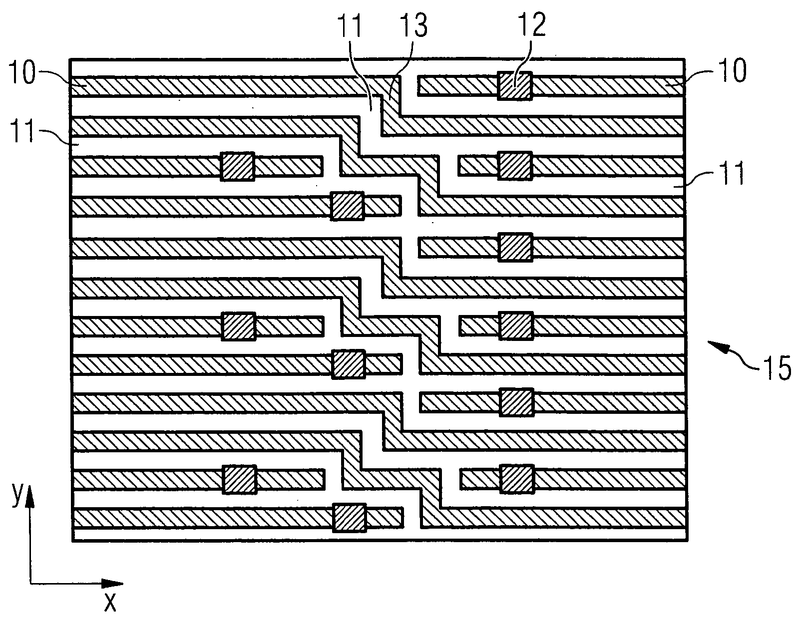
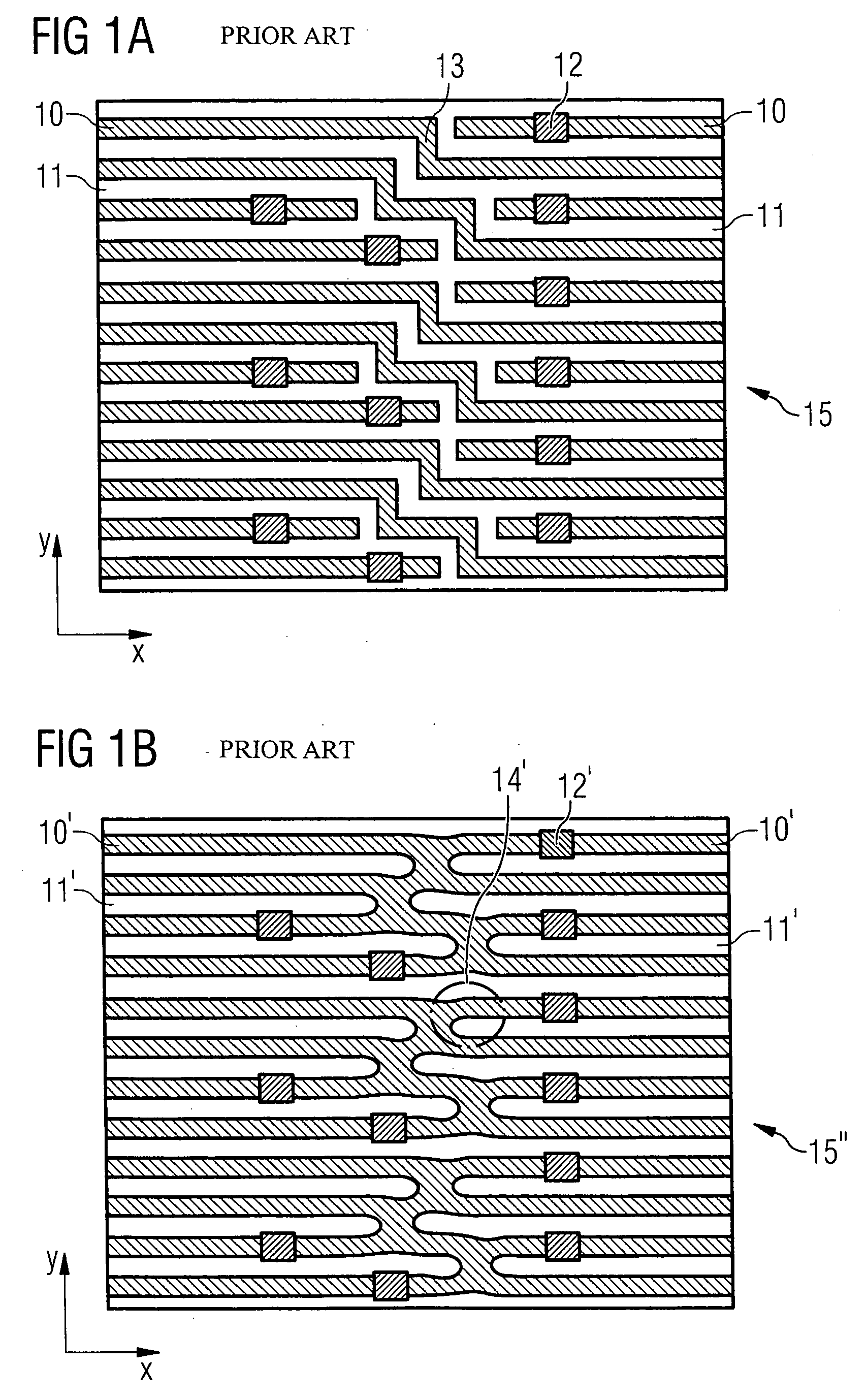
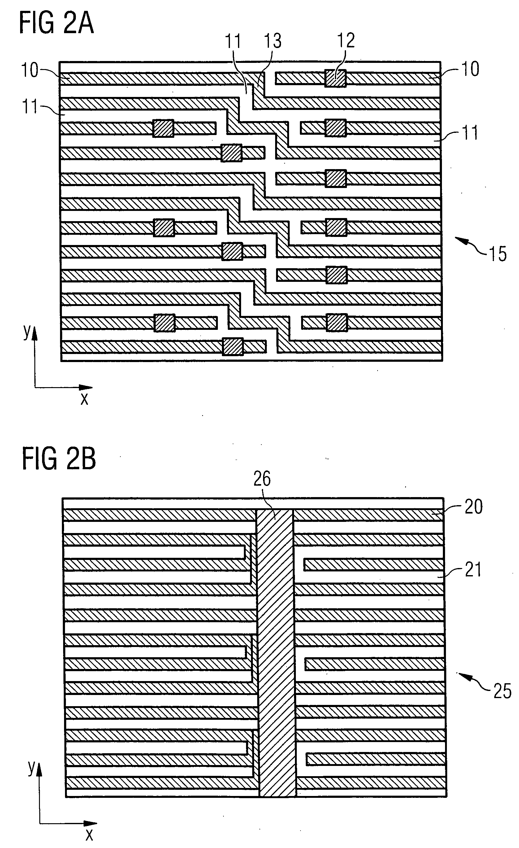
[0078]FIG. 1a shows a layout for a semiconductor circuit that consists of a number of elements, in a diagrammatic representation.

[0079] Semiconductor tracks are shown as main semiconductor patterns 10, connecting semiconductor patterns 13, contact points 12 and intermediate spaces as non-conductive areas 11.

[0080] The conductor tracks are mainly aligned along a first direction, the x direction in FIG. 1a. The x direction is the predominant imaging direction since, for producing the semiconductor circuit of FIG. 1a, a lithography mask is exposed with a dipole aperture, which achieves a particularly good imaging quality along one direction.

[0081]FIG. 3b shows such a dipole aperture 2 that includes an opaque area 2a in which two circular aperture openings 2b are left open. Only the circular apertures 2b are transparent whereas the area 2a is formed to be opaque. The axis defined by con...


PUM


Abstract

A method is used to produce semiconductor patterns (10′, 13′) on a wafer (15′). For this purpose, a mask (25) and a dipole aperture (2) with two aperture openings (2b) arranged behind one another in a dipole axis (y) are used. The mask (25) is imaged on the wafer (15′) by means of the dipole aperture (2) and, by the imaging of the mask (25) on the wafer (15′), main semiconductor patterns (10′) are produced which are aligned perpendicularly to the dipole axis (y) and in parallel with an imaging axis (x). A second mask (35) with at least one connecting mask pattern (33) is imaged on the wafer (15′) by means of a second aperture (6), as a result of which a connecting semiconductor pattern (13) is produced on the wafer (15′), by means of which at least two of the main semiconductor patterns (10′) are connected to one another.

Description

[0001] This application claims priority to German Patent Application 10 2005 003 183.3, which was filed Jan. 19, 2005, and is incorporated herein by reference. TECHNICAL FIELD [0002] The invention relates to a method for producing semiconductor patterns on a wafer. BACKGROUND [0003] It is known to produce semiconductor circuits from wafers that are exposed through a mask in such a manner that mask patterns of the mask are imaged as semiconductor patterns on the wafer. The mask patterns are usually either opaque or transparent for the light waves used in the imaging exposure. During the imaging process, the opaque mask patterns cover patterns on the wafer in such a manner that they are not illuminated. The light waves pass through transparent mask patterns during the imaging process, which is why a light incidence occurs on areas of the wafer covered by transparent mask patterns. The wafers are usually constructed in such a way that their structure changes with light incidence (for e...

Claims


Application Information

Patent Timeline
IPC IPC(8): G03F7/00
CPCG03F1/144G03F7/701G03F7/70425G03F7/70466G03F1/70
Inventor HENNIG, MARIOKOESTLER, WOLFRAMMOUKARA, MOLELATHIELE, JOERGWINKLER, THORSTENZEILER, KARSTEN
Owner INFINEON TECH AG
Why Eureka
Try Eureka