Top emission flat panel display with sensor feedback stabilization

a flat panel display and sensor technology, applied in the field of flat panel displays, can solve the problems of differential color aging over the lifetime of the display, oled material has to be restricted, and the uniformity of manufacture is not uniform

Inactive Publication Date: 2006-08-17
LEADIS TECH
View PDF4 Cites 16 Cited by
  • Summary
  • Abstract
  • Description
  • Claims
  • Application Information

AI Technical Summary

Benefits of technology

[0007] The present invention discloses novel top emitter pixel circuitry for flat panel displays. Sensor material is deposited above a substrate. A pixilated opaque cathode is deposited above the sensor material. Organic light emitting diode material is deposited above the cathode. A transparent anode is deposited above the OLED material. Some of the layers have dielectric layers between them. The light emitted by the OLED material passes upwards through the transparent anode but cannot pass downwards through the opaque cathode. A deep via optically

Problems solved by technology

The primary technical problems with the commercialization of the OLED display are manufacturing uniformity and differential color aging over the

Method used


Image

  • Top emission flat panel display with sensor feedback stabilization
  • Top emission flat panel display with sensor feedback stabilization
  • Top emission flat panel display with sensor feedback stabilization

Examples


Embodiment Construction

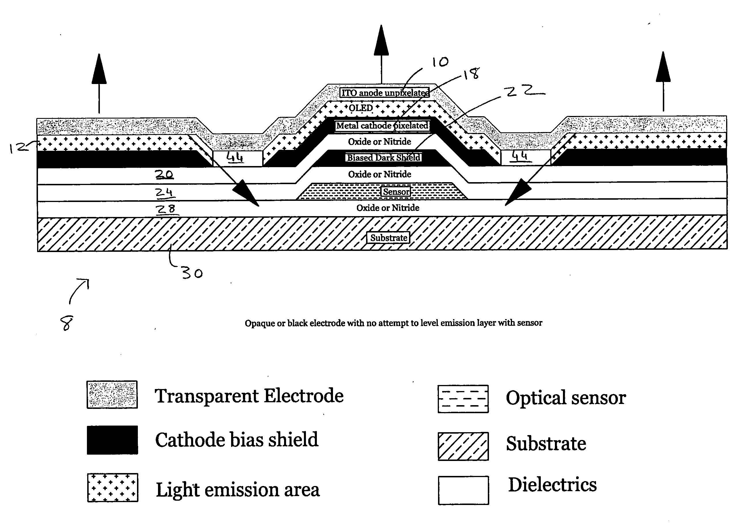
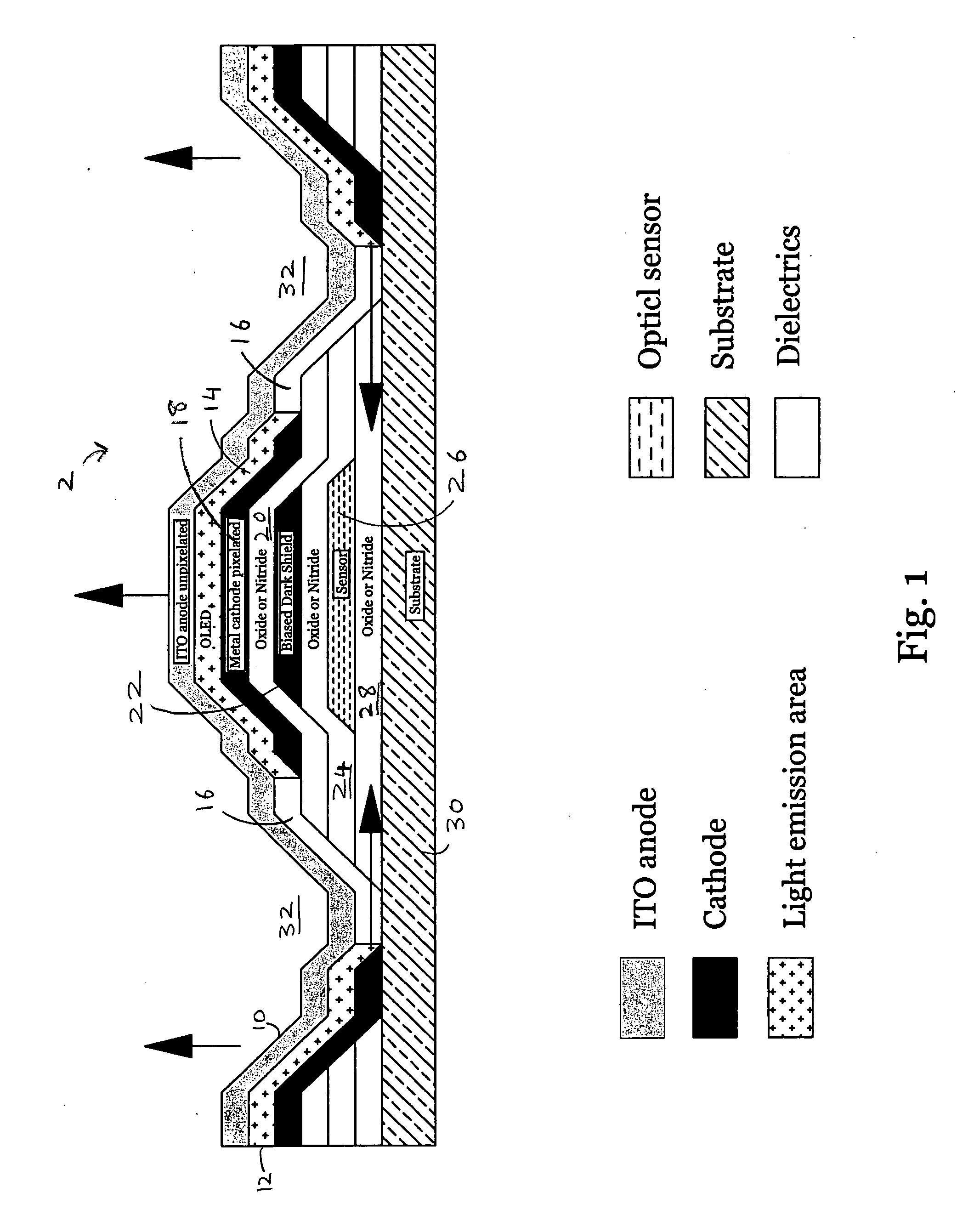
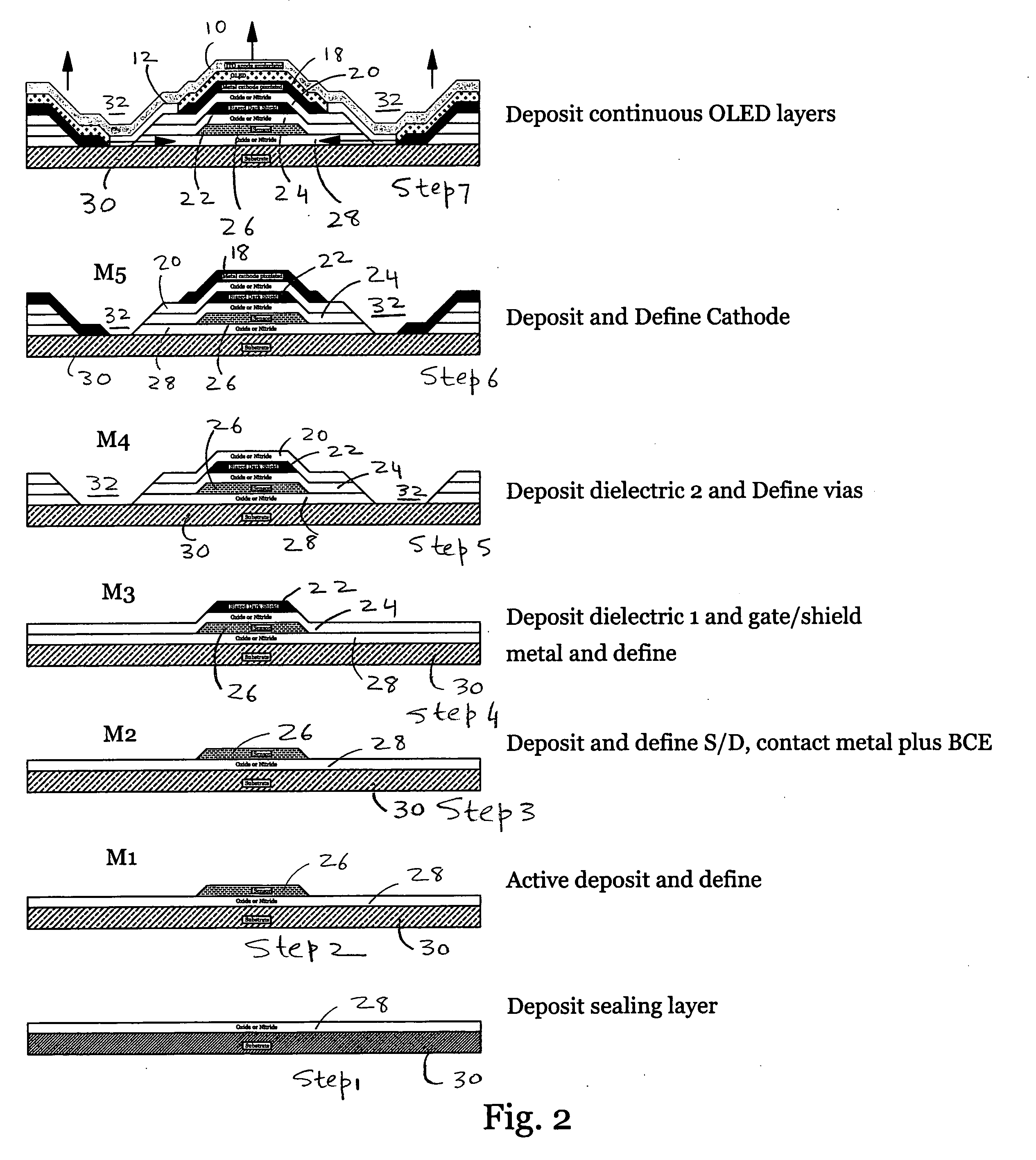
[0019] The present invention covers top emitter pixel circuitry and methods for fabricating same. The top emitter pixel circuitry of the present invention can also be referred to as the up emitter pixel circuitry. The active matrix circuitry included in the top emitter pixel circuitry of the present invention is located under the OLED emitter that has either a pixilated cathode (negative electrode) structure with a transparent anode layer (positive electrode) for the emitting surface, or has a transparent cathode as the emitting surface. In one embodiment, the cathode is opaque and pixilated. In that embodiment, a deep via is used to align the edge of the OLED emitter with the edge of the sensor.

[0020] In another embodiment, both electrodes (anode and cathode) are transparent and thus interchangeable. In that embodiment, the metal gate of the thin film transistor (TFT) of the active matrix is a top gate that is situated between the emitting OLED and the TFT channel, to shield the T...


PUM


Abstract

The present invention discloses novel top emitter pixel circuitry for flat panel displays. Sensor material is deposited above a substrate. A pixilated opaque cathode is deposited above the sensor material. Organic light emitting diode material is deposited above the cathode. A transparent anode is deposited above the OLED material. Some of the layers have dielectric layers between them. The light emitted by the OLED material passes upwards through the transparent anode but cannot pass downwards through the opaque cathode. A deep via optically connects the OLED material layer with the sensor material layer. A transparent cathode can be used instead of the opaque cathode, thereby allowing the light generated by the OLED material layer to pass both upward through the transparent anode and downward through the transparent cathode. That would eliminate the need for a deep via to form an optical path between the OLED material layer and the sensor layer. However, that would require the addition of a shield to shield the active matrix circuitry from the light generated by the OLED material layer.

Description

RELATED APPLICATION [0001] The present application claims priority to U.S. Provisional Patent Application No. 60 / 645,521, filed on Jan. 18th, 2005.FIELD OF INVENTION [0002] The present invention relates to flat panel displays. BACKGROUND OF THE INVENTION [0003] A new emissive type flat panel display technology called organic light emitting diode (OLED) is in the process of development by many companies around the world such as Sharp, Toshiba, Samsung, and many more. The primary technical problems with the commercialization of the OLED display are manufacturing uniformity and differential color aging over the lifetime of the display. These problems have been addressed by several provisional and formal patent applications assigned to the Nuelight Corporation. Refer to U.S. patent application Ser. No. 10 / 872,344 entitled Method and Apparatus for Controlling an Active Matrix Display and U.S. patent application Ser. No. 10 / 872,268 entitled Controlled Passive Display Apparatus and Method ...

Claims


Application Information

Patent Timeline
IPC IPC(8): H01L31/00
CPCH01L27/12H01L27/3269H01L27/3272H01L51/5234H01L2251/5315H01L2251/5323H10K59/13H10K59/126H10K50/828H10K2102/3031H10K2102/3026
Inventor NAUGLER, W. EDWARD JR.REDDY, DAMODERLIU, GORDON JUN
Owner LEADIS TECH
Why Eureka
Try Eureka