Method of forming metal line in semiconductor device

a metal line and semiconductor technology, applied in semiconductor/solid-state device manufacturing, basic electric elements, electric devices, etc., can solve the problems of difficult depositing and burying of metal line material, seam or void, and inability to meet the desired line width through the line formation method using an existing reactive ion etching process

Inactive Publication Date: 2006-08-24
SK HYNIX INC
View PDF3 Cites 2 Cited by
  • Summary
  • Abstract
  • Description
  • Claims
  • Application Information

AI Technical Summary

Benefits of technology

[0012] Accordingly, the present invention has been made in view of the above problems, and it is an object of the present invention to provide a method of forming a line i...

Problems solved by technology

As the line width of semiconductor devices was miniaturized and the degree of integration thereof increased, it became impossible to fulfill a desired line width through a line formation method using an existing Reactive Ion Etch (RIE) process.
It is thus difficult to deposit and bury the metal line material.
There also occurs a problem in that tungsten (W) of WF6 and the Ti film being the glue layer react to each other in an explosive manner (hereinafter, referred to as “W volcano”).
The inlet of the trench becomes narrow toward the top of the trench, thus causing a seam or void.
Furthermore, this phenomenon becomes more profound when the line structure is miniaturized, and thus causes failure i...

Method used


Image

  • Method of forming metal line in semiconductor device
  • Method of forming metal line in semiconductor device
  • Method of forming metal line in semiconductor device

Examples


Embodiment Construction

[0029] Embodiments according to the present invention will be described with reference to the accompanying drawings. Since the embodiments are provided so that a person of ordinary skill in the art will be able to understand the present invention, they may be modified in various manners and the scope of the present invention is not limited by the embodiments described herein.

[0030]FIGS. 1A to 1E are cross-sectional views showing process steps of forming a metal line in a semiconductor device according to an embodiment of the present invention.

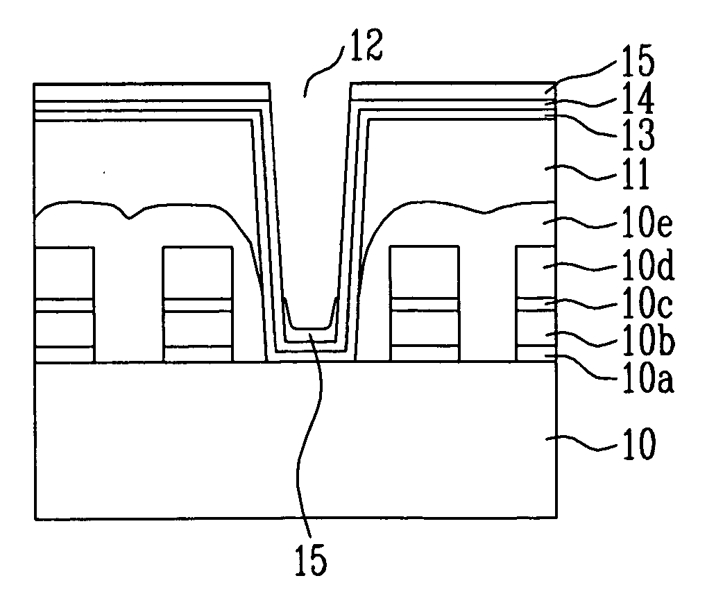
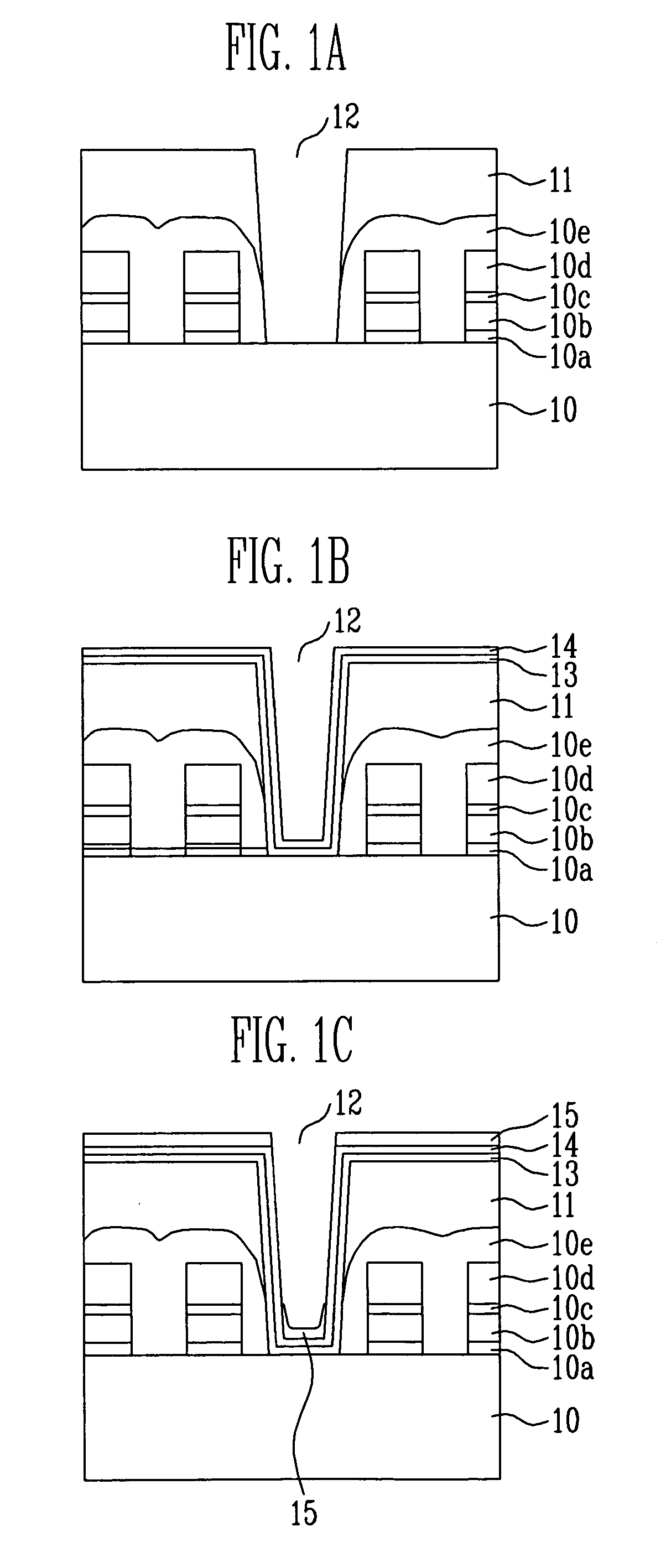
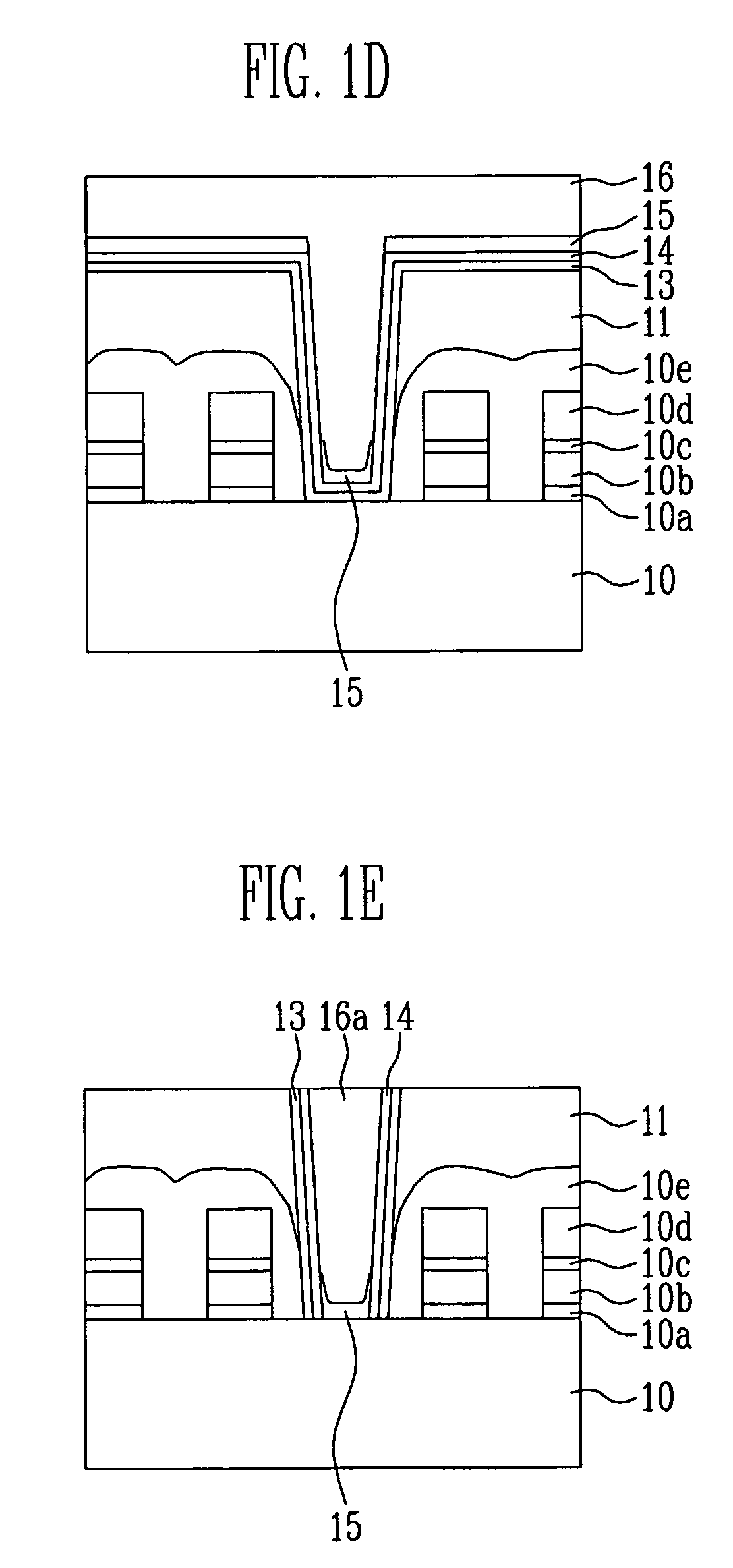
[0031] Referring first to FIG. 1A, an interlayer insulating film 11 is formed on a semiconductor substrate 10 in which predetermined structures are formed. The interlayer insulating film 11 is etched to expose a desired portion of the semiconductor substrate 10, thus forming a trench 12.

[0032] In this case, the trench 12 preferably has sides of a profile that is almost perpendicular.

[0033] The predetermined structure may have a variety of s...


PUM


Abstract

A method of forming a line a semiconductor device, including the steps of forming an interlayer insulating film on a semiconductor substrate in which predetermined structures are formed, forming a trench through which a predetermined region of the semiconductor substrate is exposed in the interlayer insulating film, sequentially forming a glue layer and a first barrier metal film on the entire surface including the trench, forming a second barrier metal film at the bottom of the trench, and forming a line within the trench.

Description

BACKGROUND [0001] 1. Field of the Invention [0002] The present invention relates to a method of forming a metal line in a semiconductor device. More specifically, the present invention relates to a method of forming a metal line of a semiconductor device, wherein line resistance of the line can be reduced, and line burial characteristics and electrical characteristics can be improved. [0003] 2. Discussion of Related Art [0004] As the line width of semiconductor devices was miniaturized and the degree of integration thereof increased, it became impossible to fulfill a desired line width through a line formation method using an existing Reactive Ion Etch (RIE) process. Recently, lines have been formed by means of a damascene method. [0005] In case of the line formation method using the damascene method, a metal line material has to be deposited / buried in a pattern region that is formed in the form of a trench, unlike the RIE method. [0006] A source contact of a NAND flash memory devic...

Claims


Application Information

Patent Timeline
IPC IPC(8): H01L21/44H01L21/4763
CPCH01L21/2855H01L21/28556H01L21/28562H01L21/76846H01L21/28
Inventor KIM, TAE KYUNGCHO, JIK HO
Owner SK HYNIX INC
Why Eureka
Try Eureka