Calibration method

a technology of calibration method and optical axis, which is applied in the direction of electrical programme control, program control, instruments, etc., can solve the problems of failure to disclose any means for adjusting the optical axis, failure to correct the setting angle by obtaining the correct alignment of the optical axis, and difficulty or impossible to visually observe the wafer in the processing apparatus or the like from the outsid

Inactive Publication Date: 2006-08-31
YASKAWA DENKI KK
View PDF2 Cites 15 Cited by
  • Summary
  • Abstract
  • Description
  • Claims
  • Application Information

AI Technical Summary

Benefits of technology

[0010] The preferred embodiments of the present invention have been developed in view of the above-mentioned and / or other problems in the related art. The preferred embodiments of the present invention can significantly improve upon existing methods and / or apparatuses.

Problems solved by technology

In some cases, however, it is very difficult or impossible to visually observe a wafer in a processing apparatus or the like from the outside.
However, the aforementioned reference fails to disclose any means for adjusting the optical axis.
Furthermore, although the misalignment of the setting angle of the hand itself will also be added as misalignment of the optical axis, no method of correcting the setting angle by obtaining the misalignment of the optical axis correctly has been proposed.

Method used


Image

  • Calibration method
  • Calibration method
  • Calibration method

Examples


Embodiment Construction

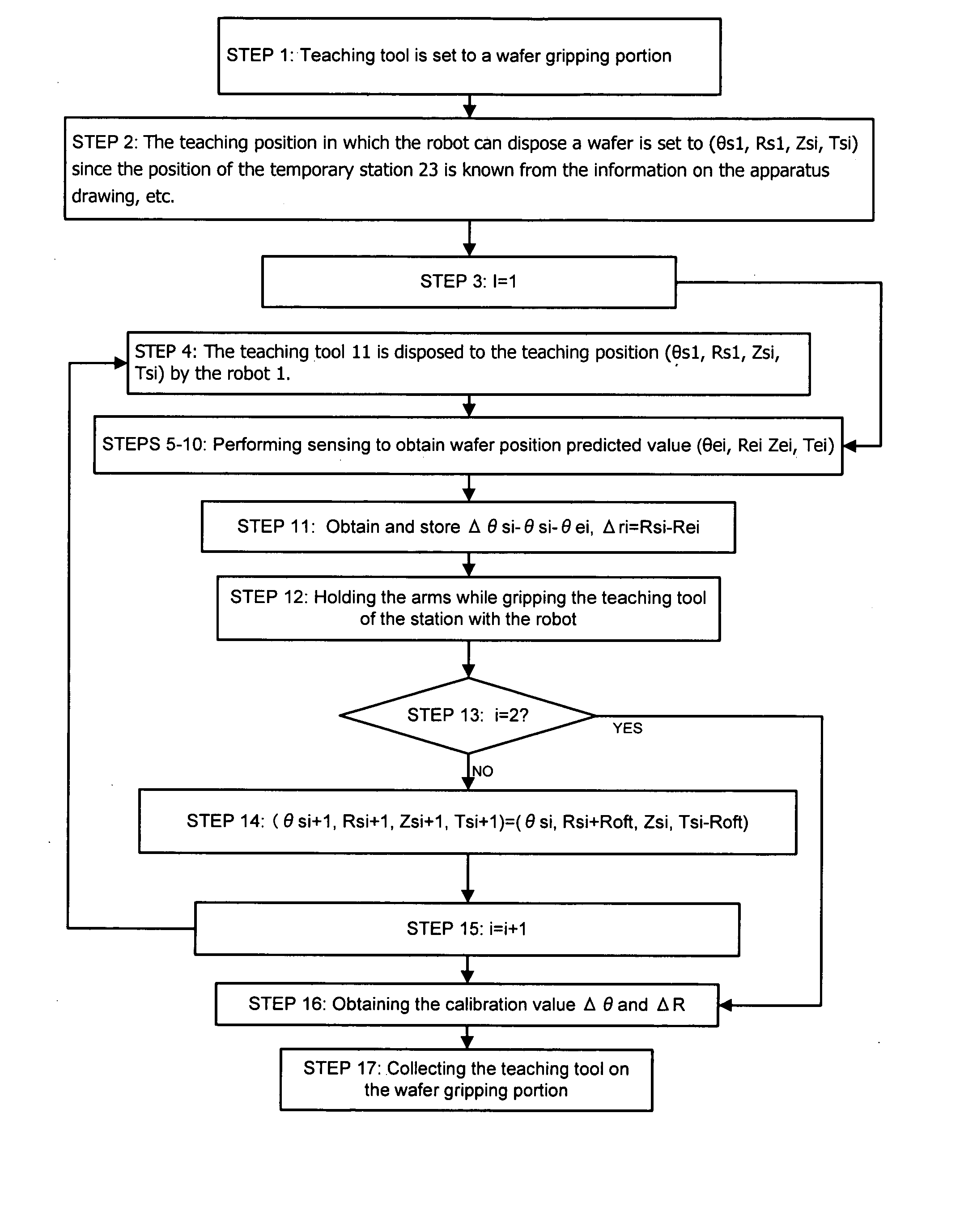
[0045] In the following paragraphs, some preferred embodiments of the invention will be described by way of example and not limitation. It should be understood based on this disclosure that various other modifications can be made by those in the art based on these illustrated embodiments.

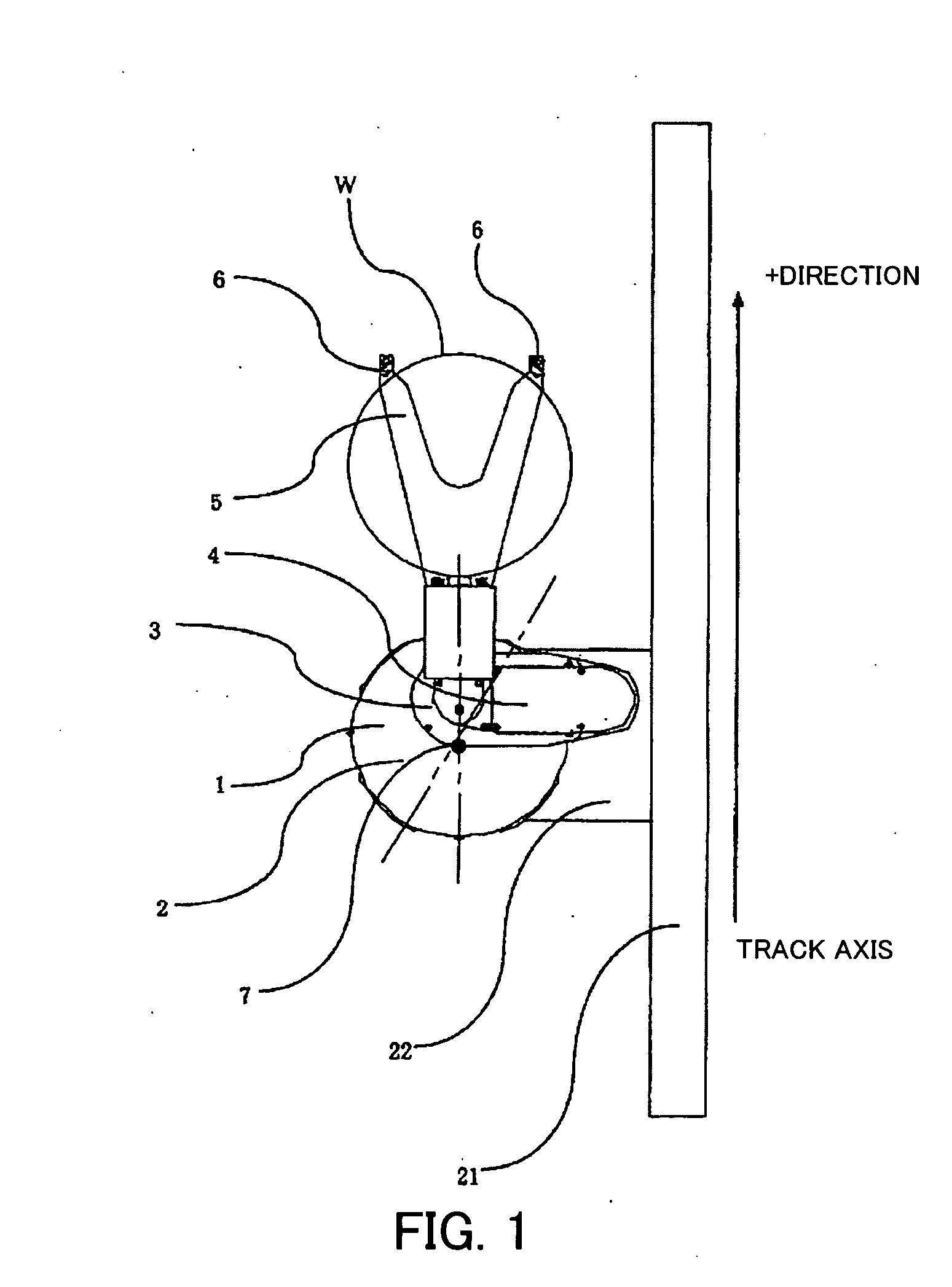
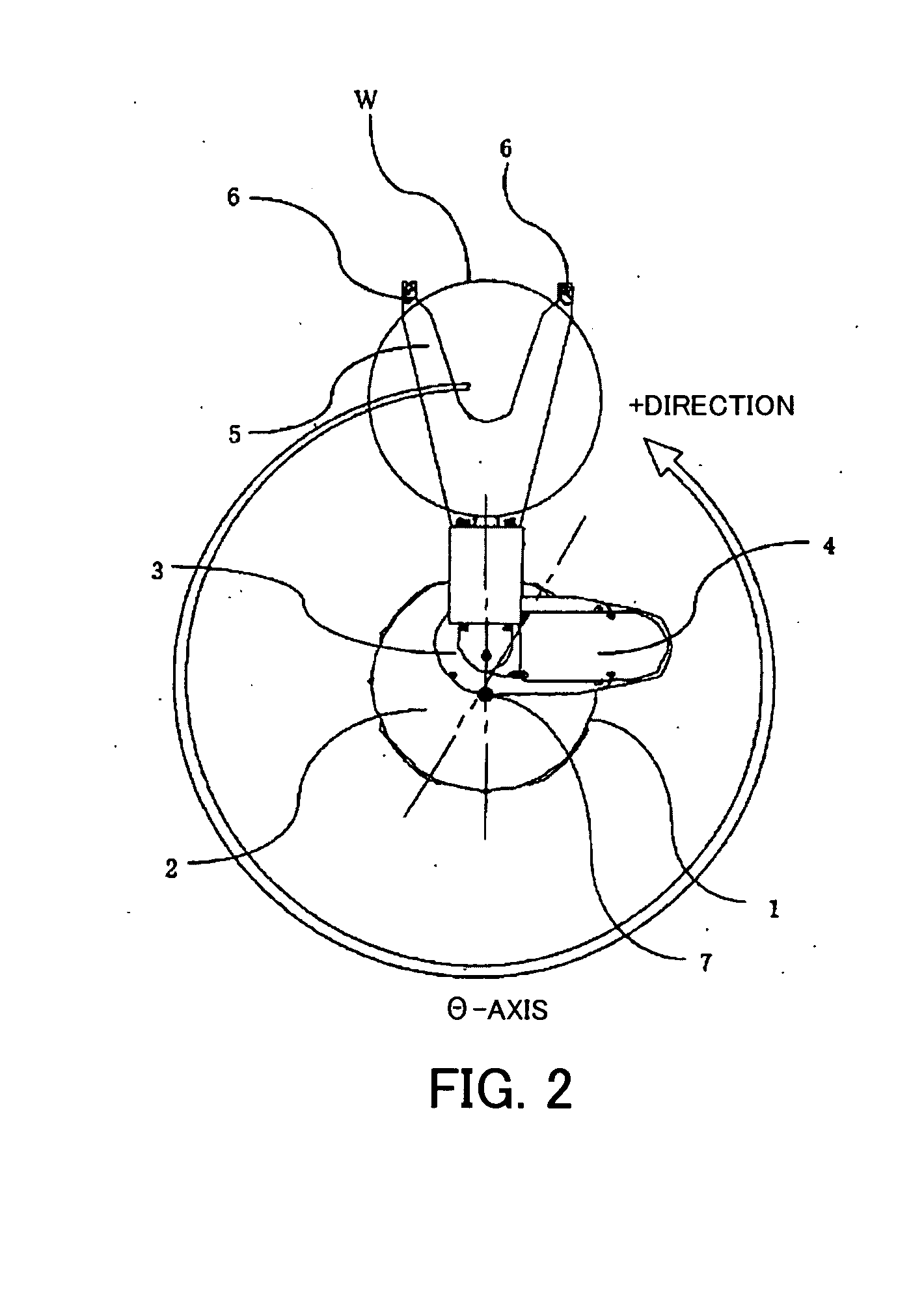
[0046] Each of FIGS. 1 to 4 is an explanatory view of a robot for use in an embodiment of the present invention, wherein FIGS. 1 to 3 are plan views thereof, and FIG. 4 is a side view thereof. In these figures, the reference numeral “1” denotes a horizontal articulated robot for carrying a semiconductor wafer, and the reference letter “W” denotes a semiconductor wafer to be carried. The robot 1 is provided with a first arm 3 capable of rotating within a horizontal plane about the robot rotation central axis 7 of the columnar supporting portion 2 configured to move up and down, a second arm 4 attached to the tip end of the first arm 3 so as to be rotated within a horizontal plane, and a wafer grippi...


PUM


Abstract

In some preferred embodiments of the present invention, a method of performing calibration of an optical axis of a sensor installed on a hand of an arm of a robot by obtaining misalignment of the optical axis of the sensor relative to the hand or by obtaining misalignment of the hand relative to the arm is provided. A method of performing calibration by detecting a teaching tool 11 disposed at a semiconductor wafer placing position of a storage container or a carrying device by a sensor 6 installed on a hand 5 of a robot 1 to teach the position of the semiconductor wafer to the robot 1 includes a step of placing the teaching tool 11 at specified position with the robot 1, a step of predicting the position of the teaching tool 11 detecting the teaching tool 11 with the sensor 6, and a step of obtaining a difference between the position of the teaching tool 11 and the predicted value.

Description

RELATED APPLICATIONS [0001] This application is a continuation-in-part of a National Stage of International Patent Application No. PCT / JP2004 / 015061, filed on Oct. 13, 2004. This application claims priority under 35 U.S.C. §119 to Japanese Patent Application No. 2003-3574600 filed on Oct. 17, 2003. Each of the entire disclosures of these applications is incorporated herein by reference in its entirety.BACKGROUND OF THE INVENTION [0002] 1. Field of the Invention [0003] The present invention relates to a calibration method, and some preferred embodiments relate to a method of calibrating an optical axis of a sensor mounted on a robot hand to teach a position of a semiconductor wafer to a semiconductor wafer carrying robot. [0004] 2. Description of Related Art [0005] The following description sets forth the inventor's knowledge of related art and problems therein and should not be construed as an admission of knowledge in the prior art. [0006] Conventionally, teaching operation of a se...

Claims


Application Information

Patent Timeline
Patent Type & Authority Applications(United States)
IPC IPC(8): G05B19/42B25J9/22G01B11/00B25J9/10B25J13/08H01L21/00H01L21/677H01L21/68
CPCH01L21/67259H01L21/67739H01L21/681B25J9/10B25J13/08H01L21/68
Inventor ADACHI, MASARUKAWABE, MITSUNORI
Owner YASKAWA DENKI KK
Why Eureka
Try Eureka