Check patentability & draft patents in minutes with Patsnap Eureka AI!

Phase-change memory device and manufacturing process thereof

a technology of phase-change memory and manufacturing process, which is applied in the direction of solid-state devices, transistors, electrical apparatus, etc., can solve the problem of not being able to implement all the currently available processes

Inactive Publication Date: 2006-09-14
STMICROELECTRONICS SRL
View PDF10 Cites 46 Cited by
  • Summary
  • Abstract
  • Description
  • Claims
  • Application Information

AI Technical Summary

Benefits of technology

[0024] an array of memory cells arranged in rows and columns and each including a MOS selection device and a phase-change region connected to the selection device, the selection device having a first conductive region and a second co

Problems solved by technology

The structure of FIG. 2 has the disadvantage that it cannot be implemented with all the currently available processes, in particular when the basic CMOS technology does not enable local interconnections of an LIL type to be made.

Method used


Image

  • Phase-change memory device and manufacturing process thereof
  • Phase-change memory device and manufacturing process thereof
  • Phase-change memory device and manufacturing process thereof

Examples


Embodiment Construction

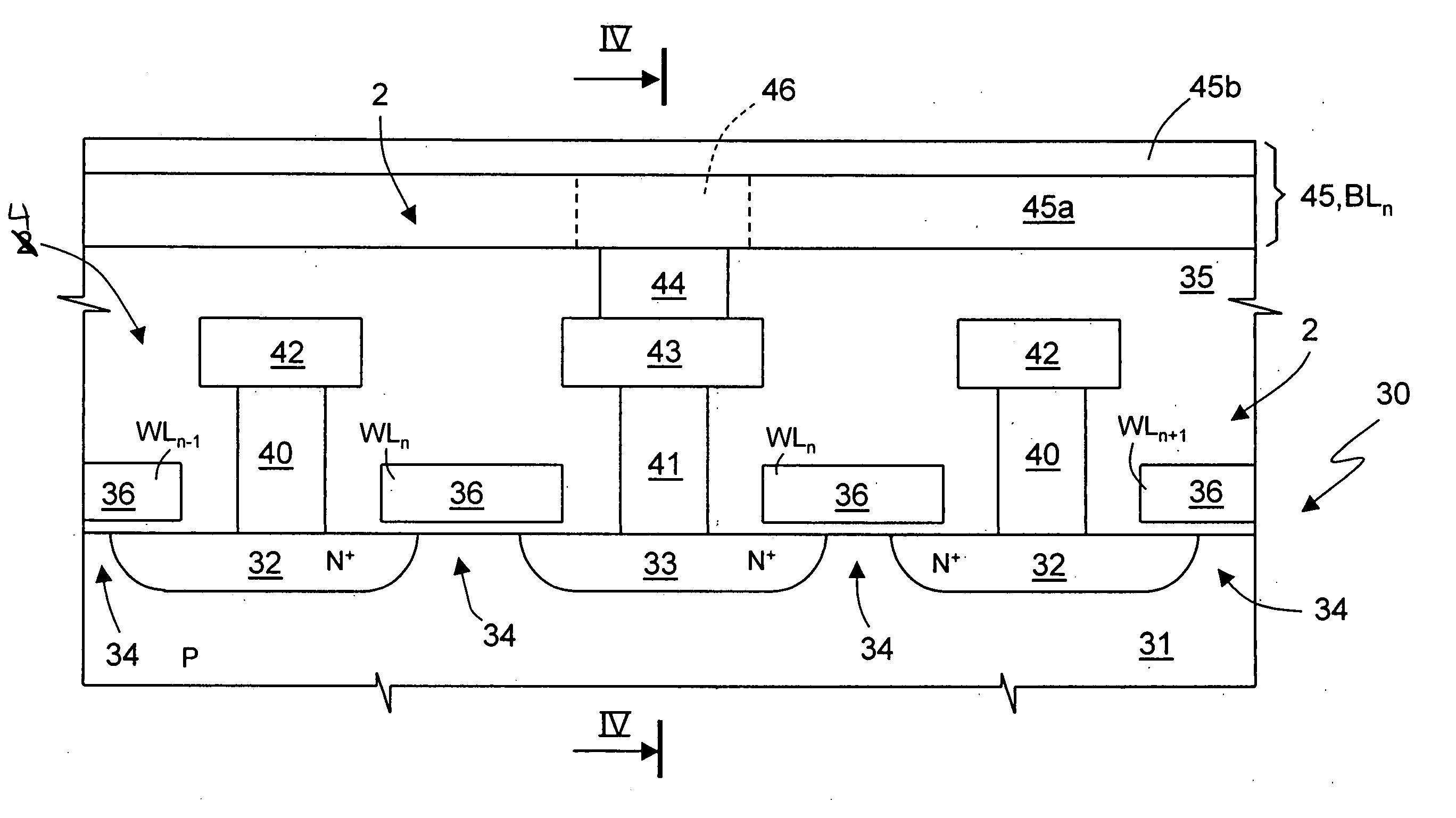
[0035]FIGS. 3-5 refer to an embodiment wherein the source line is made in a metal layer, and precisely in the first metal level (meta11). Furthermore, the bitline is formed on top of the first metal level, and precisely between the first and second metal levels (not illustrated). Furthermore, the memory cells are split-gate cells, i.e., the selection element 4 is formed by two MOS transistors connected in parallel and thus equivalent to an individual MOS transistor having a width W twice the width of the defined active area.

[0036] In detail, a wafer 30 comprises a substrate 31 of a P type accommodating source regions 32 (two of which are visible in FIG. 3) and drain regions 33 (just one of which is visible in FIG. 3). Between each source region 32 and the adjacent drain region 33, the substrate 31 forms a channel region 34; a dielectric layer 35 coats all the surface of the substrate 31 and accommodates gate regions 36 that extend on the channel regions 34 and are formed by polysil...


PUM


Abstract

A phase-change memory device, wherein memory cells form a memory array arranged in rows and columns. The memory cells are formed by a MOS selection device and a phase-change region connected to the selection device. The selection device is formed by first and second conductive regions which extend in a semiconductor substrate and are spaced from one another via a channel region, and by an isolated control region connected to a respective row and overlying the channel region. The first conductive region is connected to a connection line extending parallel to the rows, the second conductive region is connected to the phase-change region, and the phase-change region is connected to a respective column. The first connection line is a metal interconnection line and is connected to the first conductive region via a source-contact region made as point contact and distinct from the first connection line.

Description

BACKGROUND OF THE INVENTION [0001] 1. Field of the Invention [0002] The present invention relates to a phase-change memory (PCM) device and the manufacturing process thereof. [0003] 2. Description of the Related Art [0004] As is known, phase-change memory devices are based upon storage elements which use a class of materials that have the property of switching between two phases having distinct electrical characteristics, associated to two different crystallographic structures of the material forming the storage element, namely a disorderly amorphous phase and an orderly crystalline or polycrystalline phase. [0005] Currently, the alloys of the elements of group VI of the periodic table, such as Te or Se, referred to as calcogenides or calcogenic materials, may be advantageously used in phase-change memory cells. The currently most promising calcogenide is formed by an alloy of Ge, Sb, and Te (Ge2Sb2Te5), which is now widely used for storing information in over-writable disks. [0006]...

Claims


Application Information

Patent Timeline
IPC IPC(8): H01L29/94
CPCH01L45/06H01L45/1233H01L45/126H01L45/144H01L27/2436H01L27/2472H10B63/82H10B63/30H10N70/231H10N70/8413H10N70/826H10N70/8828
Inventor ZULIANI, PAOLAPELLIZZER, FABIOBEZ, ROBERTO
Owner STMICROELECTRONICS SRL
Features
  • R&D
  • Intellectual Property
  • Life Sciences
  • Materials
  • Tech Scout
  • Unparalleled Data Quality
  • Higher Quality Content
  • 60% Fewer Hallucinations
Learn More