

Flexible liquid crystal display and manufacturing method of the same
a liquid crystal display and flexible technology, applied in the field of liquid crystal display, can solve the problems of distorted image, difficult to maintain uniform cell gap, and inability to display required image,
- Summary
- Abstract
- Description
- Claims
- Application Information
AI Technical Summary
Benefits of technology
Problems solved by technology
Method used
Image


Examples
first embodiment
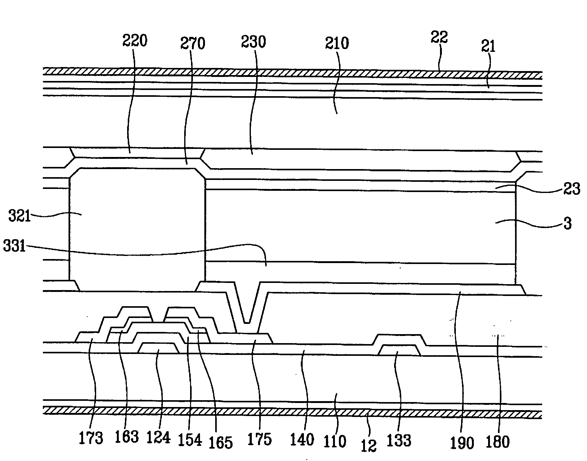
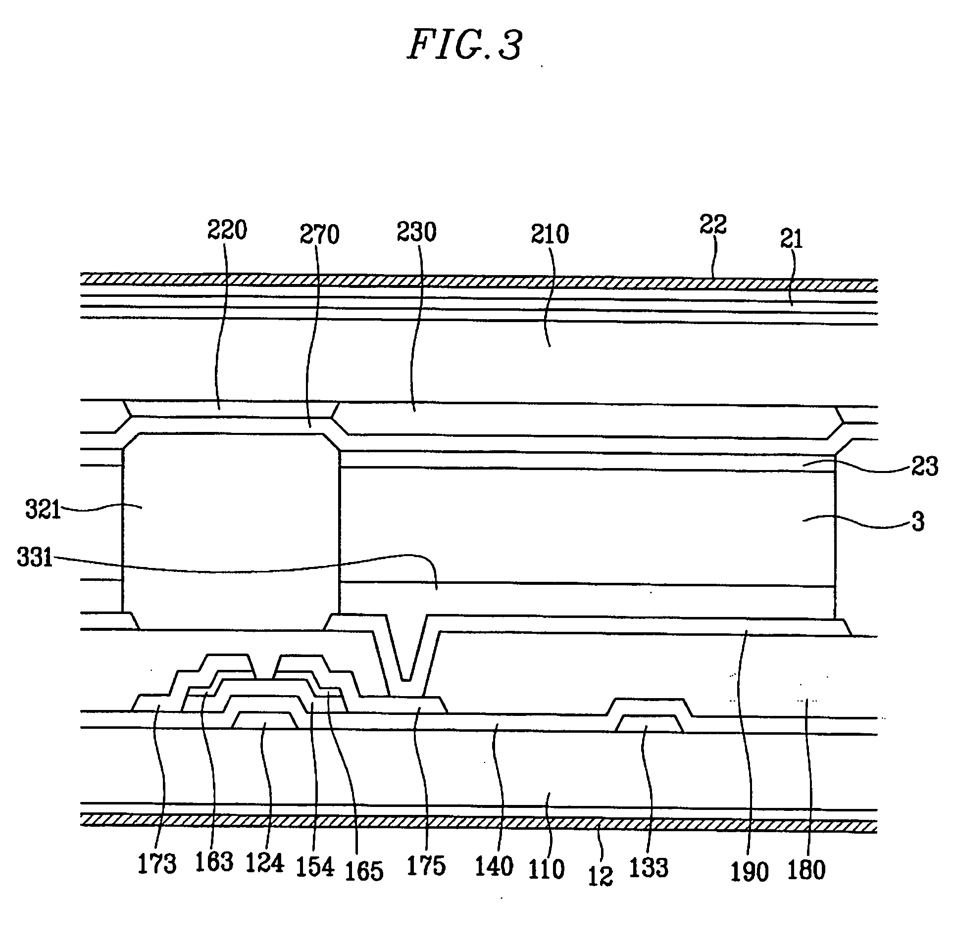
[0041] Hereinafter, an LCD according to the invention is described with reference to FIG. 1 and FIG. 2.
[0042]FIG. 1 is a perspective view of an LCD and FIG. 2 is a perspective view showing the state of a spacer formed on a common electrode panel used in the LCD shown in FIG. 1.
[0043] Referring to FIG. 1, a spacer 321, e.g., lattice-shaped, is arranged between an upper insulating substrate 110 and a lower insulating substrate 210 with a common electrode 270. A high-molecular weight layer 331 is arranged on an inner surface of the upper substrate 110.
[0044] The spacer 321 maintains a space (referred to as a cell gap) between the two substrates 110 and 210, and partitions the space into a plurality of regions. As shown in FIG. 1, each region may correspond to a pixel unit or a combination of pixel units. The regions are filled with nematic liquid crystal 3.
[0045] The spacer 321 may be formed using a photolithography process. For example, after the lower substrate 210 is coated with ...
second embodiment
[0088]FIG. 12 is a perspective view of an LCD according to the invention. FIG. 13 is a perspective view showing the condition of a spacer arranged on a common electrode panel used in the LCD shown in FIG. 12.
[0089] Referring to FIG. 12, an upper insulating substrate 110 and a lower insulating substrate 210 with a common electrode 270 are arranged to face each other, and a plurality of bar-shaped spacers 322 are arranged parallel to each other between the upper substrate 110 and the lower substrate 210. Linearly formed high molecular weight projections 332 are crossed with the spacers 322 between the upper substrate 110 and the lower substrate 210.
[0090] According to such structure, the spacer 322 defines and maintains a substantially fixed space between the upper substrate 110 and the lower substrate 210. The space is partitioned into a plurality of regions by an intersection of the spacers 322 and the high molecular weight projections 332. Each region may correspond to a pixel uni...
third embodiment
[0117]FIG. 24 is a perspective view of an LCD according to the invention.
[0118] This LCD of the third embodiment further includes a high molecular weight layer formed on an inner surface of the upper substrate 110, together with the high-molecular projections 332, compared with the structure shown in FIG. 12.
[0119] Such a structure is obtained by performing UV irradiation multiple times, e.g., twice. For example, the first UV irradiation is performed to form the high molecular weight projections 332 using a photo-mask with slits, and the second UV irradiation is performed to separate the remaining monomer from the liquid crystal after the formation of the high molecular weight projections 332.
[0120] As described above, the monomer is mixed with the liquid crystal prior to the photo-polymerization. After mixing, UV irradiation is performed to form the high molecular weight layer. This high molecular weight layer attaches or adheres the spacer to the substrates. In such a structured...
PUM
| Property | Measurement | Unit |
|---|---|---|
| Phase separation | aaaaa | aaaaa |
| Pressure | aaaaa | aaaaa |
| Flexibility | aaaaa | aaaaa |
Abstract
Description
Claims
Application Information