Semiconductor memory device with three dimensional solid electrolyte structure, and manufacturing method thereof

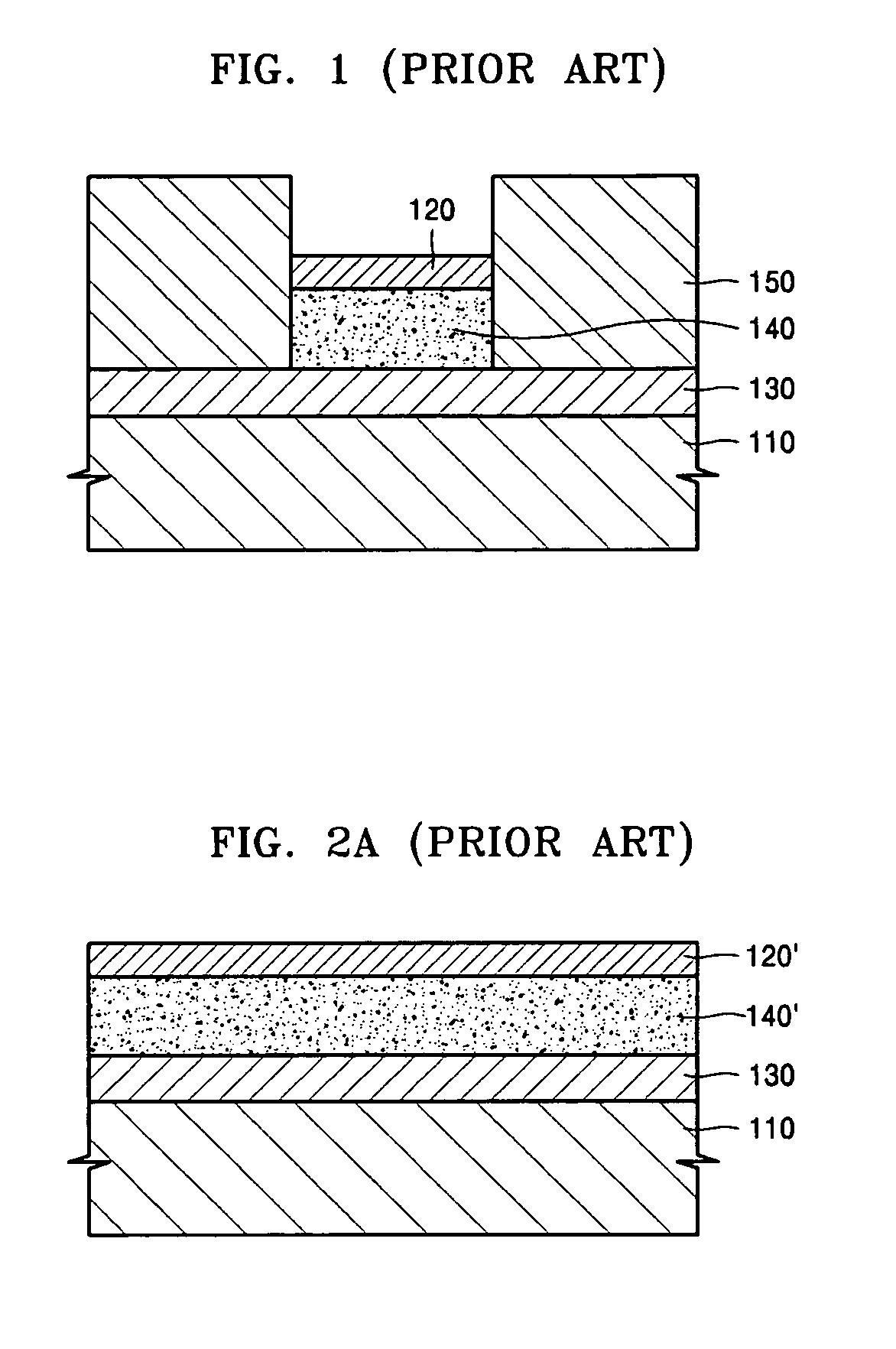
a memory device and solid electrolyte technology, applied in the direction of digital storage, capacitors, instruments, etc., can solve the problems of large heat generated in storing or erasing information, the variable resistance structure illustrated in fig. 1 cannot be miniaturized to the size currently required, and it is difficult to manufacture the variable resistance structure in the size desired by the mark

Inactive Publication Date: 2006-09-21
SAMSUNG ELECTRONICS CO LTD
View PDF12 Cites 27 Cited by
  • Summary
  • Abstract
  • Description
  • Claims
  • Application Information

AI Technical Summary

Benefits of technology

[0017] The first electrode may be formed on the substrate to provide a planarized upper surface, and the second electrode may be formed on the solid electrolyte and fill the region with a low height to provide a planarized upper surface The semiconductor memory cell using variable resistance device may include: a variable resistance device, one end of which is connected to a bit line; and a transistor having a drain connected to the other end of the variable resistance device, a source to which a reference voltage is applied, and a gate connected to a word line. The memory cell according to the present disclosure can be biased using, for example, a select transistor or a diode transistor.
[0018] Also, the semiconductor memory cell using the variable resistance device may include: a variable resistance device, one end of which is connected to a bit line; and a diode transistor having an anode connected to the other end of the variable resistance device and a cathode connected to a word line.
[0019] In addition, the semiconductor memory cell using the variable resistance device may include: a memory cell array comprising a plurality of bit lines and a plurality of word lines arranged in a matrix, and a plurality of memory cells, one end of which is connected to a corresponding bit line among the plurality of bit lines and the other end of which is connected to a corresponding word line among the plurality of word lines; and a bias circuit which biases at least one of the word lines selected from the plurality of word lines with a predetermined voltage level for a predetermined period of time.
[0020] A multibit semiconductor memory device using electric properties of the variable resistance device having a solid electrolyte having at least two regions with different heights may be provided. The exemplary multibit semiconductor memory device includes a bias circuit which supplies current at one of at least two different levels to a selected memory cell. The bias circuit may supply a current for one of the at least two different periods of time or may supply a current at one of the at least two levels for a predetermined period of time.
[0021] According to another aspect of the present invention, there is provided a manufacturing method of a variable resistance device. The exemplary method includes: forming an insulating layer on a substrate and then forming a through-hole in the insulating layer to expose a predetermined portion of the top surface of the substrate; forming a flat first electrode composed of a conductive material at the base of the through-hole; forming a solid electrolyte layer to a predetermined thickness along the outline of the through-hole using an atomic layer deposition (ALD) method so that a region with a low height is formed at the center of the solid electrolyte; forming a second electrode composed of a conductive material filling the region with the low height of the solid electrolyte so that the top surface of the surface of the resultant structure is planar; and removing part of the solid electrolyte and second electrode outside of the through-hole.
[0022] According to another aspect of the present invention, there is provided a manufacturing method of a semiconductor cell. The exemplary method includes: providing a substrate with word lines and transistors formed thereon; forming a variable resistance device so that drains of the transistors and a first electrode of the variable resistance device contact each other; and forming bit lines perpendicular to the word line such that the bit lines contact the second electrode.

Problems solved by technology

Thus, much heat is generated in storing or erasing information.
However, the variable resistance structure illustrated in FIG. 1 cannot be miniaturized to a size presently required. FIGS. 2A and 2B are views of a method of forming the programmable microelectronic structure illustrated in FIG. 1.
Since a typical solid electrolyte and an etchant have over-etched widths of about 10 nm or greater, it is difficult to manufacture the variable resistance structure in the size desired by the market.
In addition, the possibility of damage to the sides of the stacked structure during an etching process increases.
In more detail, the sides of the components become nonuniform, and thus it is difficult to obtain desirable electrical properties.

Method used


Image

  • Semiconductor memory device with three dimensional solid electrolyte structure, and manufacturing method thereof
  • Semiconductor memory device with three dimensional solid electrolyte structure, and manufacturing method thereof
  • Semiconductor memory device with three dimensional solid electrolyte structure, and manufacturing method thereof

Examples


Embodiment Construction

[0031] The present invention will now be described more fully with reference to the accompanying drawings, in which exemplary embodiments of the invention are shown. Like reference numerals in the drawings denote like elements.

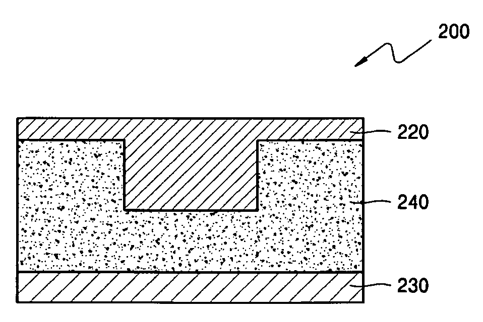
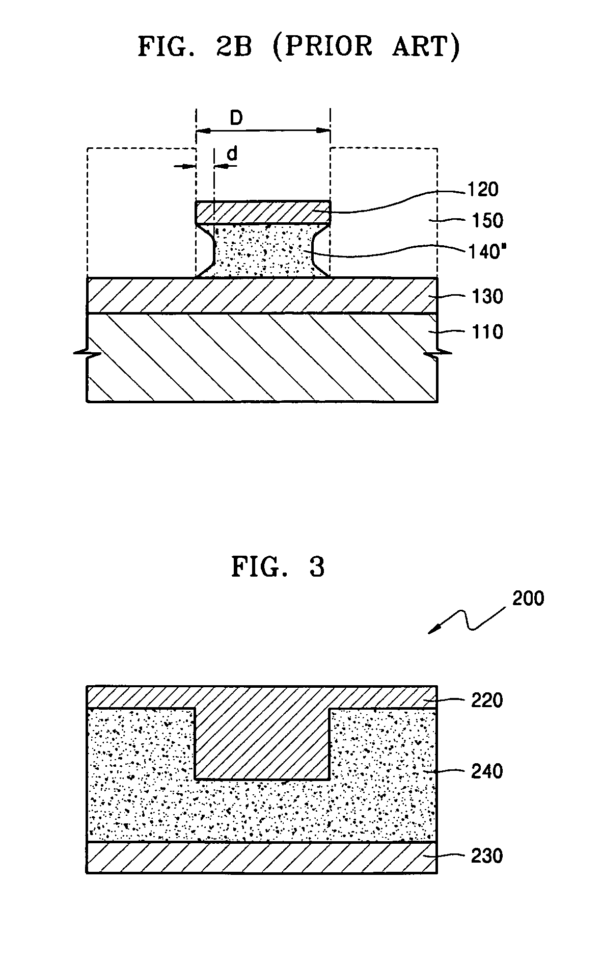
[0032]FIG. 3 is a cross-sectional view of a variable resistance device 200 according to an embodiment of the present invention. The variable resistance device 200, which can be used in a semiconductor memory, includes a first electrode 230, a second electrode 220, and a three-dimensional solid electrolyte 240 interposed between the first and second electrodes 230 and 220. The first and second electrodes 230 and 220 are made of conductive materials such as metal, and the solid electrolyte 240 has two regions. The height of the solid electrolyte 240 is the distance between the first and second electrodes 230 and 220 filled with the solid electrolyte 240.

[0033] The variable resistance device 200 may be shaped in a block, and a region of the solid electrolyte 24...


PUM


Abstract

The semiconductor memory device includes a variable resistance device having a solid electrolyte in a three-dimensional structure. The variable resistance device includes a first electrode; the solid electrolyte, which has at least two regions with different heights, formed on the first electrode; and a second electrode made of a conductive material formed on the solid electrolyte to cover the regions with different heights. In addition, a multibit semiconductor memory device is provided which includes a bias circuit that can control the intensity of a current and time the current is supplied to the variable resistance device inside a memory cell in multiple steps to configure multibits.

Description

[0001] Priority is claimed to Korean Patent Application No. 10-2005-0021844, filed on Mar. 16, 2005 in the Korean Intellectual Property Office, the disclosure of which is incorporated herein in its entirety by reference. [0002] 1. Field of the Disclosure [0003] The present disclosure relates to a semiconductor memory device, and more particularly, to a semiconductor memory device capable of storing multi-bit information by including a variable resistance device with a solid electrolyte in a 3D structure in a storage node. [0004] 2. Description of the Related Art [0005] Generally, variable resistance devices are devices in which a resistance changes according to conditions. In a conventional phase-change random access memory (PRAM), which is one type of a nonvolatile memory, a variable resistance device with a phase change material such as GST (Ge—Sb—Te), which has a resistance that varies according to a phase change caused by a change in temperature, is used. [0006] In the PRAM, the...

Claims


Application Information

Patent Timeline
Patent Type & Authority Applications(United States)
IPC IPC(8): H01G9/00
CPCG11C11/56G11C13/0009G11C2213/71G11C2213/72G11C2213/79H01C7/006H01L27/2409H01L27/2436H01L45/085H01L45/1233H01L45/1273H01L45/143H01L45/144H01L45/1616H10B63/20H10B63/30H10N70/245H10N70/8418H10N70/8825H10N70/023H10N70/826H10N70/8828
Inventor LEE, JUNG-HYUNKIM, KYU-SIK
Owner SAMSUNG ELECTRONICS CO LTD
Why Eureka
Try Eureka