Run level address mapping table and related method of construction

a mapping table and address technology, applied in the field of memory devices and memory systems, can solve the problems of high implementation cost, difficult to use flash memory as a main memory, and difficult for flash memory to use general hard disk filing systems, and achieve the effect of small memory capacity and efficient mapping information managemen

Active Publication Date: 2006-09-21
SAMSUNG ELECTRONICS CO LTD
View PDF5 Cites 51 Cited by
  • Summary
  • Abstract
  • Description
  • Claims
  • Application Information

AI Technical Summary

Benefits of technology

[0012] Embodiments of the invention are directed to a run level address mapping table and a method of forming a run level address mapping table that substantially obviates one or more limitations and / or disadvantages associated with conventional address mapping tables. For example, embodiments of the invention provide a method of forming an address mapping table enabling efficient mapping information management using only a small memory capacity.

Problems solved by technology

This characteristic makes it difficult to use flash memory as a main memory.
It also makes it difficult for flash memory to use general hard disk filing systems even in applications where flash memory is used as an auxiliary memory.
Page-level address mapping provides excellent performance because it converts an address with greater accuracy, but it is expensive to implement because it requires a large-sized address mapping table.
Block-level address mapping requires a relatively smaller sized address mapping table because only roughly converts an address, but it is expensive to manage because it must erase and update a whole data block even when only a single page in the block requires update.
In addition, block-level address mapping may undesirably break data consistency when a fault occurs during its operation.
Thus, the log-block scheme generally involves a complex process of controlling I / O operations using such tables.
However, use of these conventional address mapping methods fails to prevent an increase in the size of the address mapping table tending to result from increased data storage capacities for emerging host devices.

Method used


Image

  • Run level address mapping table and related method of construction
  • Run level address mapping table and related method of construction
  • Run level address mapping table and related method of construction

Examples


Embodiment Construction

[0022] Several embodiments of the invention will now be described as teaching examples with reference to the accompanying drawings. However, the invention is not limited to only the exemplary embodiments. Rather, the scope of the invention is defined by the claims that follow.

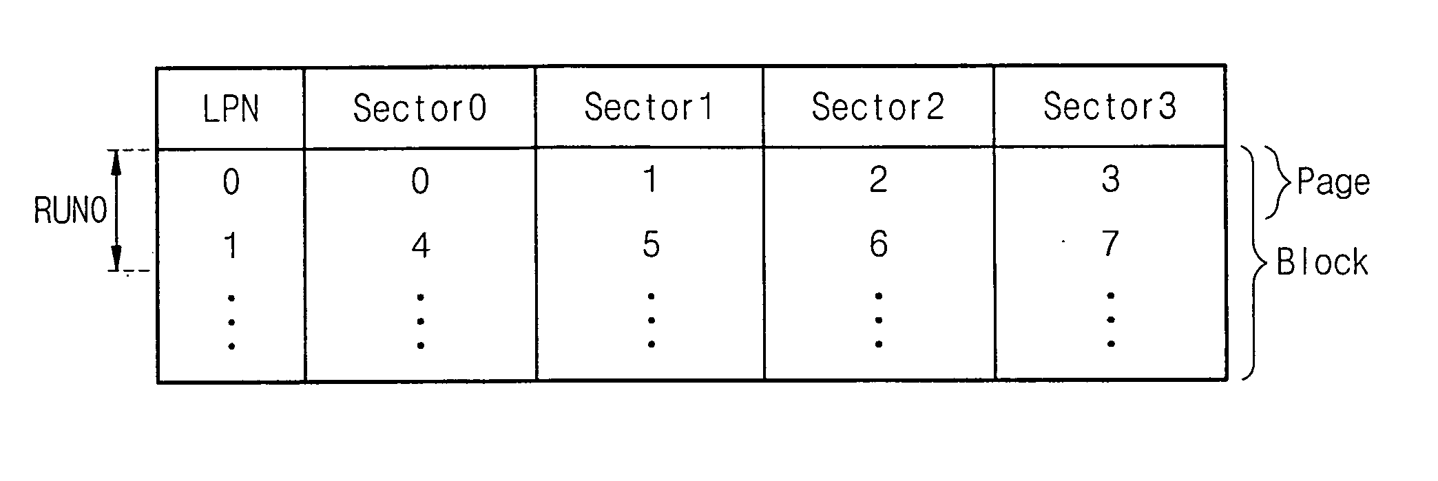
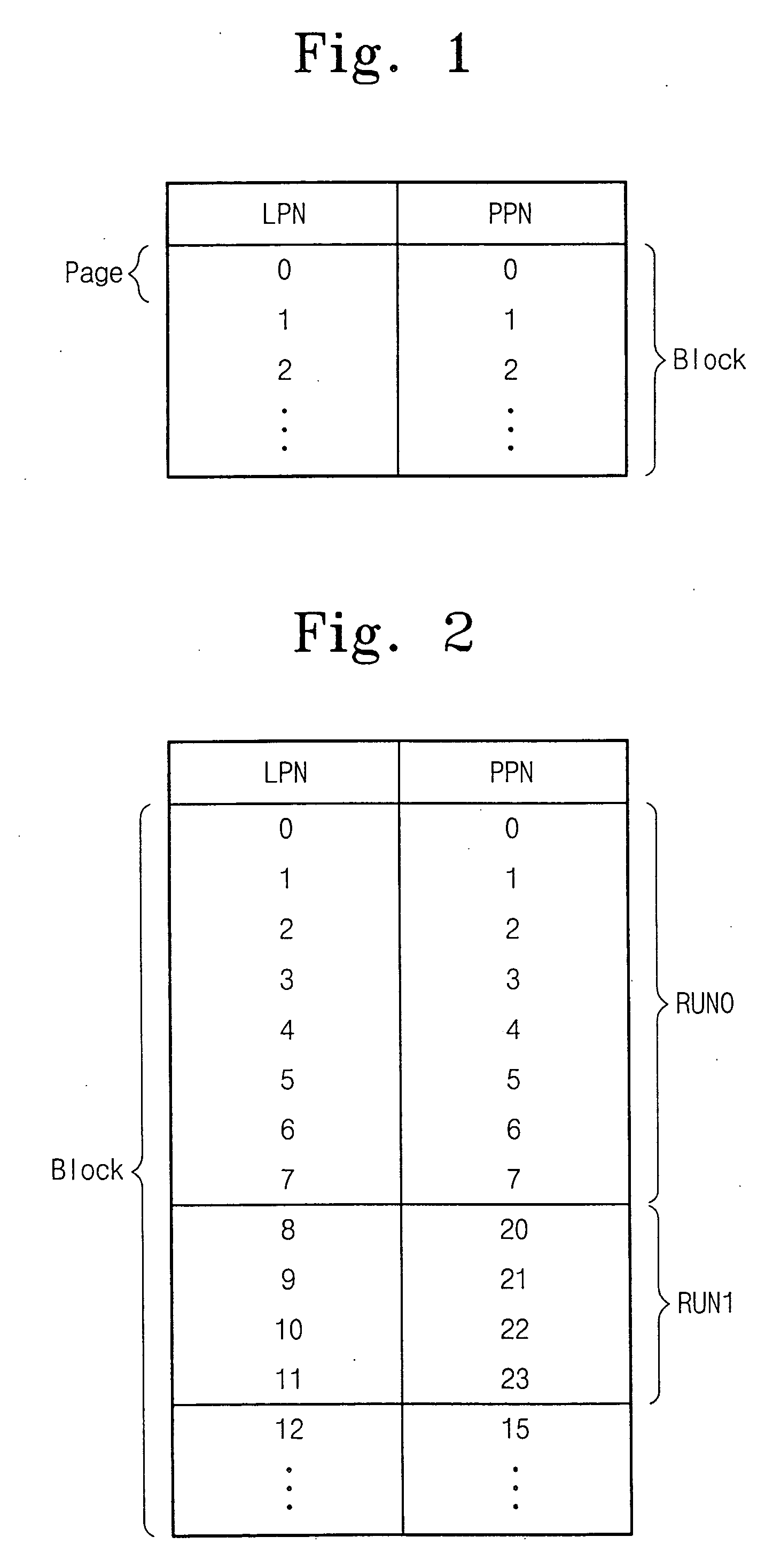
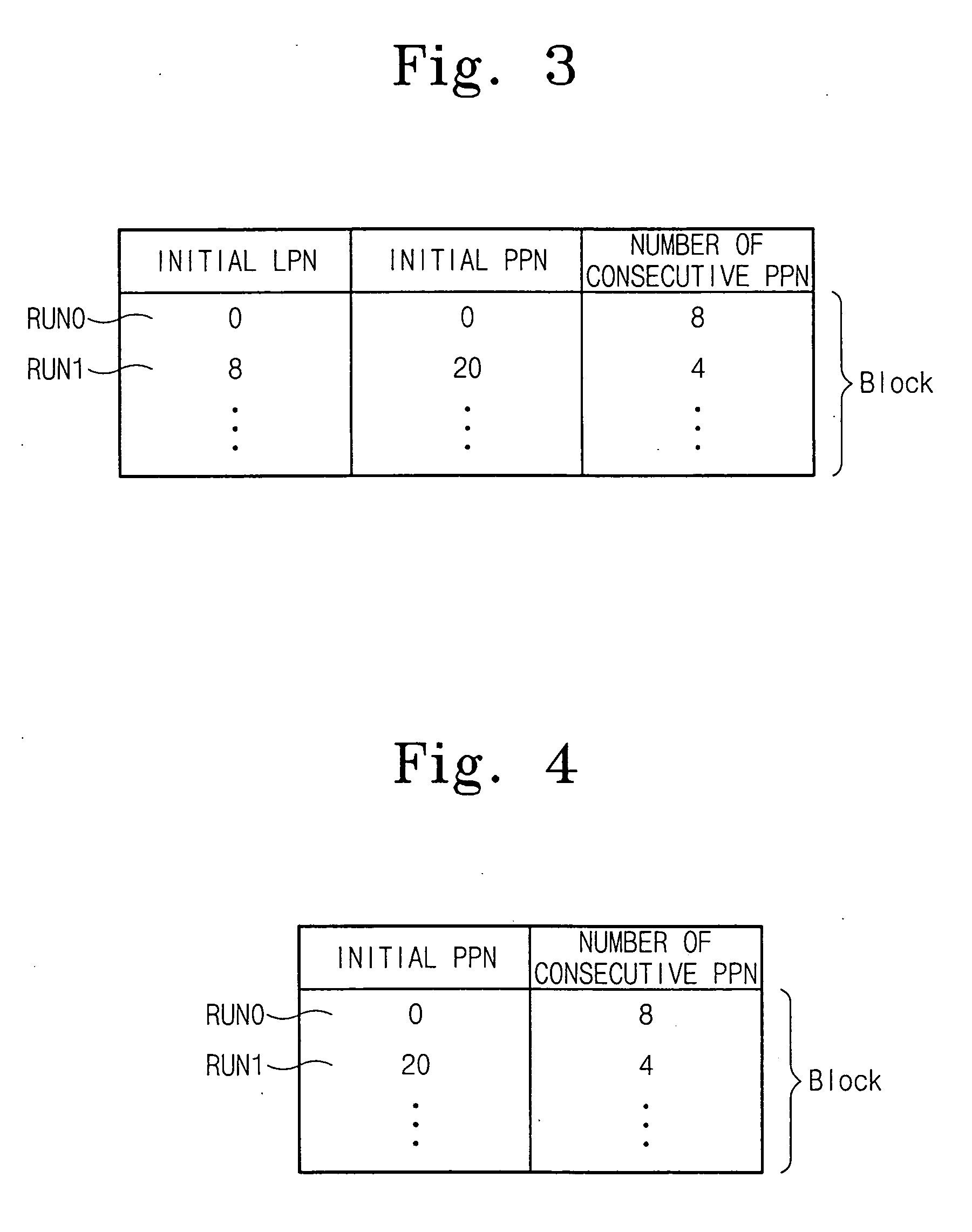
[0023] One or more embodiments of the invention provide a run level address mapping table and related method of construction. One exemplary method, constructs the address mapping table on a run basis. Here, the term “run” denotes a set of consecutive memory pages having consecutive logical and / or physical addresses. The run level address mapping table stores an initial physical page number for each run and the number of the consecutive physical pages. By doing so, the run level address mapping table makes it possible to detect all of the logical and physical page numbers contained in a run using a simple arithmetic operation. Accordingly, it is possible to efficiently manage the address mapping information usi...


PUM


Abstract

A run level address mapping table and related method of construction is disclosed. The address mapping table is constructed on a run basis, e.g., a group of consecutive pages having consecutive logical or physical addresses. The run level address mapping table stores only an initial physical page number of each run and the number of the consecutive physical pages.

Description

BACKGROUND OF THE INVENTION [0001] 1. Field of the Invention [0002] Embodiments of the invention relate generally to memory devices and memory systems. More particularly, embodiments of the invention relate to devices and methods adapted to efficiently manage nonvolatile memory, such as a flash memory. [0003] 2. Description of the Related Art [0004] A nonvolatile memory maintains data previously written to its constituent memory cell even when the memory does not receive power. Flash memory is one specific type of nonvolatile memory which is widely used in computers, memory cards, etc. Flash memory is a preferred memory choice in many applications because its memory cells may be electrically erased in bulk manner. More recently, flash memory has found increasing use on such portable information devices as cell phones, PDAs, and digital cameras. More generally, flash memory is being used with increasing frequency as a replacement for hard disk and other types of data storage. [0005] ...

Claims


Application Information

Patent Timeline
Patent Type & Authority Applications(United States)
IPC IPC(8): G06F12/10G06F12/00
CPCG06F12/0246B60P3/30A62C31/02A62C27/00A01M17/002A01M7/006B60Y2200/146
Inventor CHUNG, HYUN-MOKIM, HYE-YOUNGPARK, CHAN-IK
Owner SAMSUNG ELECTRONICS CO LTD
Why Eureka
Try Eureka