

Polymeric gate dielectrics for organic thin film transistors and methods of making the same
a thin film transistor and polymer gate technology, applied in transistors, thermoelectric devices, solid-state devices, etc., can solve the problems of amorphous silicon still having its drawbacks, amorphous silicon still has its drawbacks, and limited application of amorphous silicon to low-speed devices
- Summary
- Abstract
- Description
- Claims
- Application Information
AI Technical Summary
Benefits of technology
Problems solved by technology
Method used
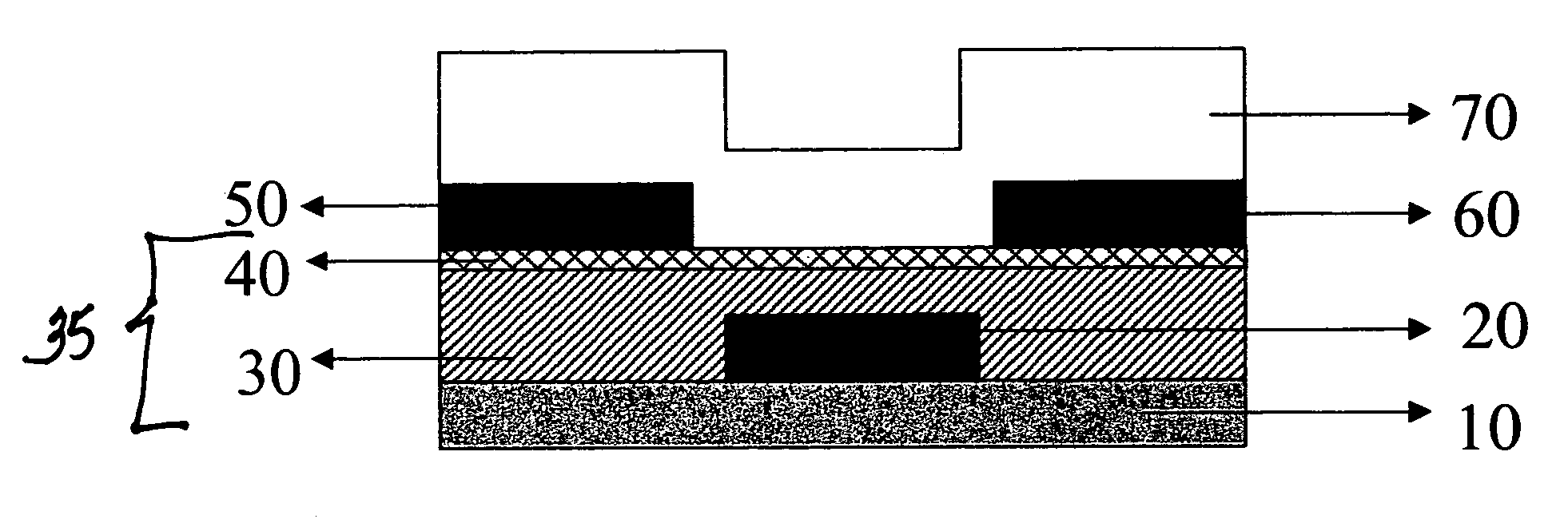
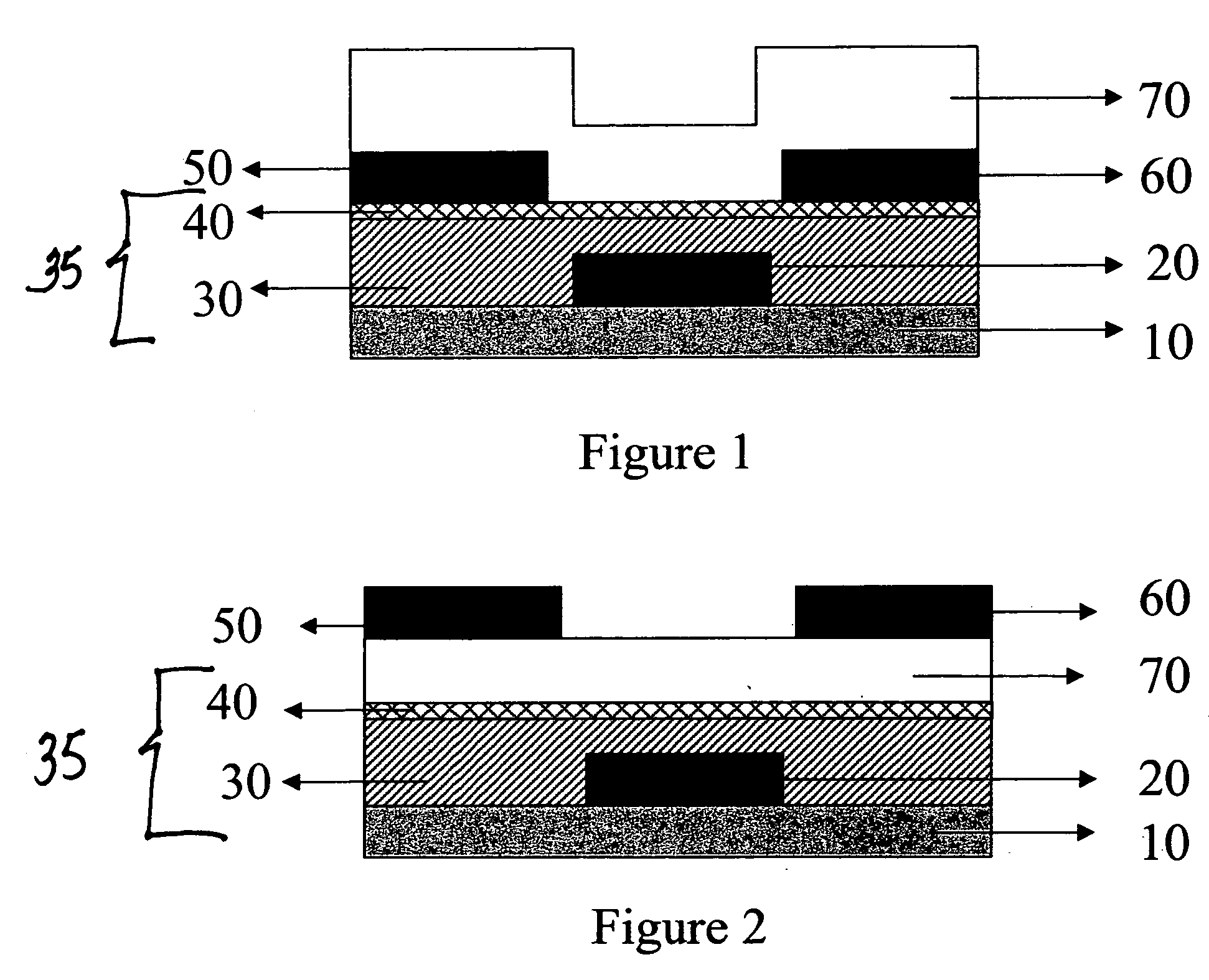
Image


Examples
examples
A. Materials:
[0068] The substrates used in the examples were single crystal orientation silicon wafers from MEMC Electronic Materials, Inc. (St. Peters, Mo.), which were heavily doped with Antimony, the wafer having a resistivity between 0.008 to 0.025 ohm / sq. Poly(4-vinylphenol), Mw˜20,000, poly(melamine-co-formnaldehyde) methylated, Mn˜511, polystyrene (secondary standard) Mn˜120,000, poly(l-vinylnaphthlene), Mn˜100,000, propylene glycol methyl ether acetate (PGMEA), as solvent, and pentacene, as a semiconductor material, were obtained from Aldrich Chemicals, Milwaukee, Wis. (Mw indicates weight average molecular weight and Mn indicates number average molecular weight. Unless otherwise indicated, the molecular weights refer to average molecular weight.)
B. Device Preparation
[0069] The wafer substrates were cleaned with Piranha solution (1 / 3 ratio of H2O2 / H2SO4 mixture) for 10 min and rinsed thoroughly with high purity water. Then, the wafers were further cleaned with UV / ozone...
PUM
 Abstract
Description
Claims
Application Information