Silicide process utilizing pre-amorphization implant and second spacer
a technology of silicon silicide and implant, which is applied in the direction of semiconductor devices, electrical equipment, transistors, etc., can solve the problems of flawed titanium silicide process
- Summary
- Abstract
- Description
- Claims
- Application Information
AI Technical Summary
Problems solved by technology
Method used
Image
Examples
Embodiment Construction
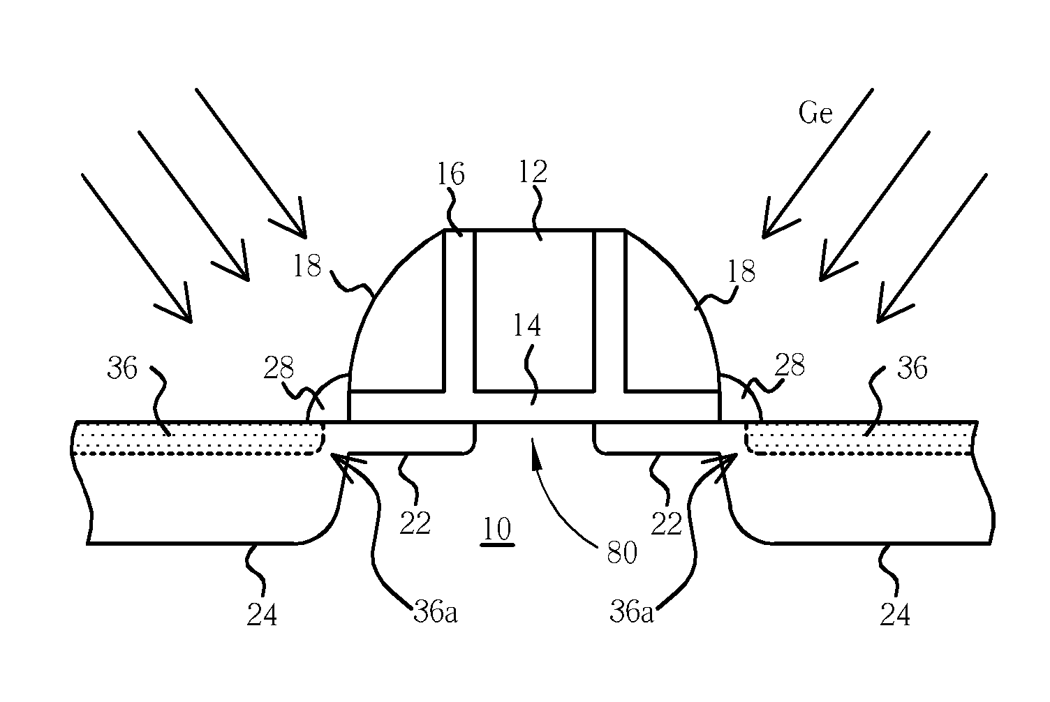
[0026] The present invention is directed to a silicide process utilizing pre-amorphization implant (PAI) and a second spacer. The advantages include: (1) the extension dopant deactivation is minimized since less area of the extension region is amorphized, thus the device performance can be improved; (2) the second spacer can avoid the nickel silicide piping effect.
[0027]FIGS. 5-10 are schematic, cross-sectional diagrams showing the improved nickel silicide process according to one preferred embodiment of the present invention. As shown in FIG. 5, a gate electrode 12 is formed over a substrate 10 such as a P type silicon substrate, with a gate oxide layer 14 therebetween.
[0028] As shown in FIG. 6, a lining layer 15, preferably a silicon dioxide layer, is then deposited over the top surface and sidewalls of the gate electrode 12, and on the exposed surface of the substrate 10. The thickness of the lining layer 15 typically ranges between 50 angstroms and 400 angstroms, but not limit...
PUM
 Abstract
Description
Claims
Application Information
 - R&D
- Intellectual Property
- Life Sciences
- Materials
- Tech Scout
- Unparalleled Data Quality
- Higher Quality Content
- 60% Fewer Hallucinations
Browse by: Latest US Patents, China's latest patents, Technical Efficacy Thesaurus, Application Domain, Technology Topic, Popular Technical Reports.
© 2025 PatSnap. All rights reserved.Legal|Privacy policy|Modern Slavery Act Transparency Statement|Sitemap|About US| Contact US: help@patsnap.com


