Molybdenum sputtering targets

a molybdenum sputtering target and molybdenum technology, applied in the field of molybdenum sputtering target, can solve the problems of non-uniform film deposited on substrates and devices, non-uniform molybdenum microstructure, and wrought microstructure, and achieve the effect of improving performance and high purity

Inactive Publication Date: 2006-03-02
H C STARCK INC
View PDF4 Cites 85 Cited by
  • Summary
  • Abstract
  • Description
  • Claims
  • Application Information

AI Technical Summary

Benefits of technology

[0009] The present invention is directed to molybdenum, sputtering targets characterized as having no or minimal texture banding or through thickness gradient. The molybdenum sputtering targets having a fine, uniform grain size as well as uniform texture, have high purity and can be micro-alloyed to improved performance.

Problems solved by technology

In many cases, sputtering targets, particularly those containing molybdenum, have a wrought microstructure with non-uniform grain texture, which may change from one sputtering target to the next.
These “non-uniformities” lead to non-uniform films being deposited onto substrates and devices, particularly flat panel displays that do not operate optimally.
Unfortunately, this methodology generally induces heterogeneity of grain size and texture.
The heterogeneity in the sputtering targets typically leads to sputtered films that do not possess the uniformity desired in most semiconductor and photoelectric applications.
The preparation of segmented plates requires an increased amount of machining and assembly cost compared to the production of a single plate ingot.
Additionally, the assembly of different plates creates variability in the large segmented plate, which can cause unacceptable variability in films formed by sputtering the large plate target.

Method used


Image

  • Molybdenum sputtering targets
  • Molybdenum sputtering targets
  • Molybdenum sputtering targets

Examples


Embodiment Construction

[0054] Other than in the operating examples or where otherwise indicated, all numbers or expressions referring to quantities of ingredients, reaction conditions, etc., used in the specification and claims are to be understood as modified in all instances by the term “about.” Various numerical ranges are disclosed in this patent application. Because these ranges are continuous, they include every value between the minimum and maximum values. Unless expressly indicated otherwise, the various numerical ranges specified in this application are approximations.

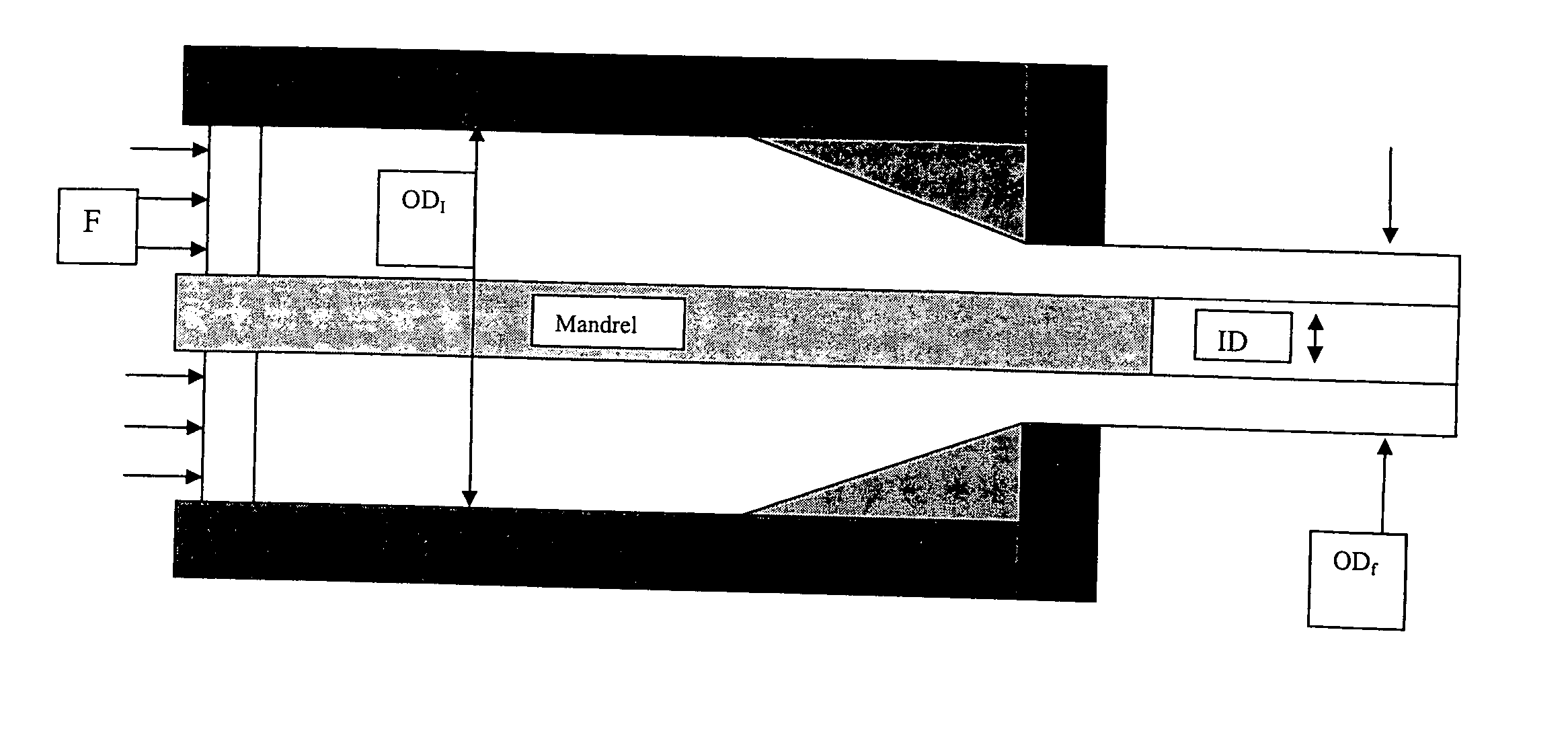
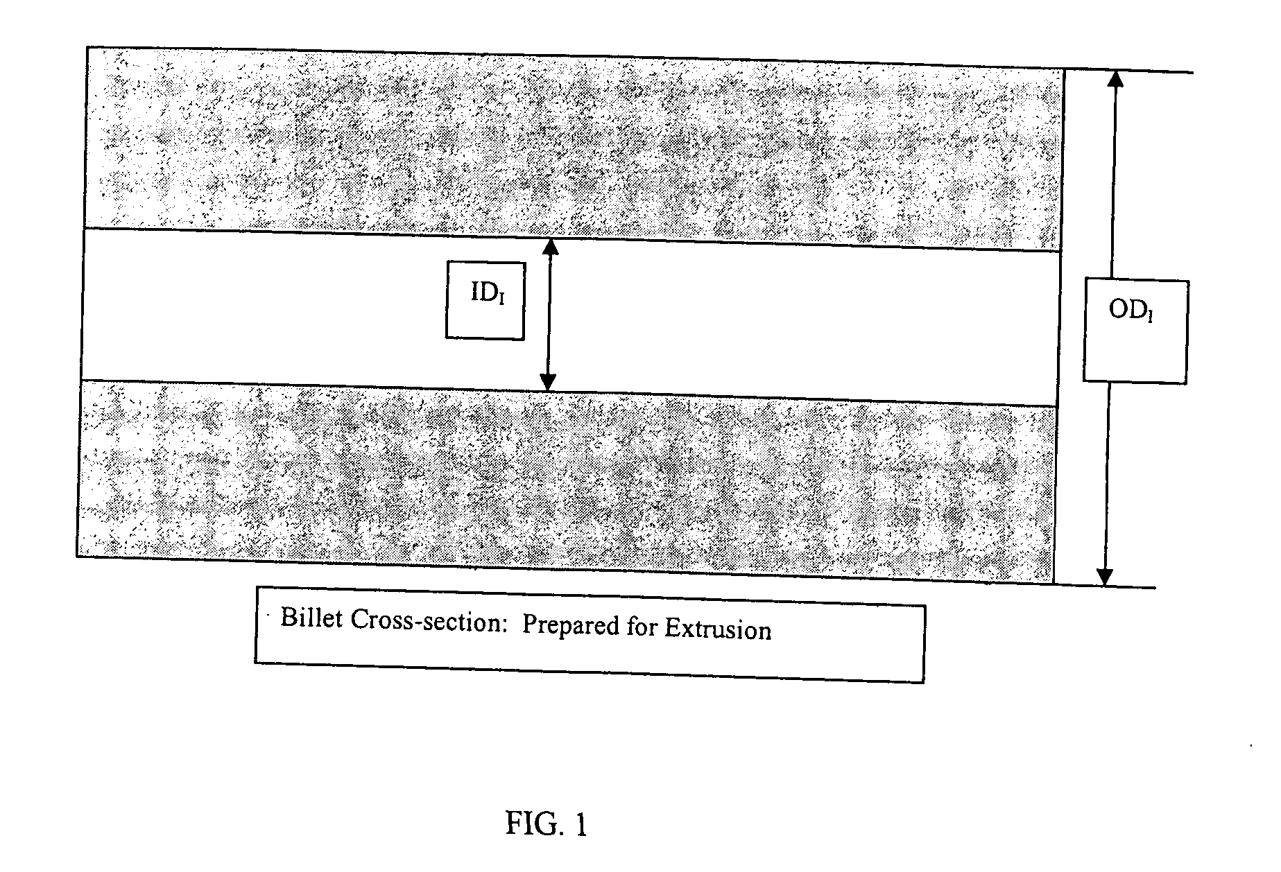
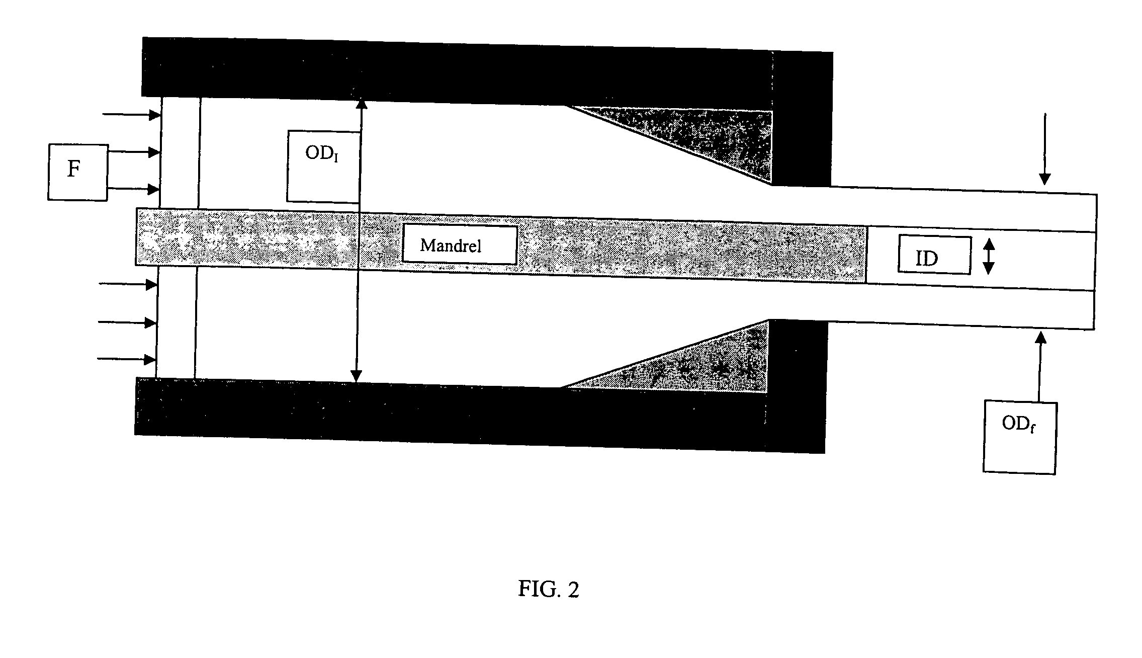
[0055] As used herein, the term “banding” refers to non-uniformities in the grain or texture, the grain size, or grain orientation that occur in a strip or pattern along the surface of the sputtering target. As used herein, the term “through thickness gradient” refers to changes in grain or texture, grain size, or grain orientation moving from the edge of the target to the center of the target.

[0056] The forms of molybdenum, sputt...


PUM

PropertyMeasurementUnit
grain sizeaaaaaaaaaa

Abstract

Molybdenum, sputtering targets and sintering characterized as having no or minimal texture banding or through thickness gradient. The molybdenum sputtering targets having a fine, uniform grain size as well as uniform texture, are high purity and can be micro-alloyed to improved performance. The sputtering targets can be round discs, square, rectangular or tubular and can be sputtered to form thin films on substrates. By using a segment-forming method, the size of the sputtering target can be up to 6 m×5.5 m. The thin films can be used in electronic components such as Thin Film Transistor—Liquid Crystal Displays, Plasma Display Panels, Organic Light Emitting Diodes, Inorganic Light Emitting Diode Displays, Field Emission Displays, solar cells, sensors, semiconductor devices, and gate device for CMOS (complementary metal oxide semiconductor) with tunable work functions.

Description

TECHNICAL FIELD OF THE INVENTION [0001] The present invention relates to forms of molybdenum, their use as sputtering targets and method of their manufacture. BACKGROUND OF THE INVENTION [0002] The sputtering technique is a film-forming technique with which a plasma is utilized to generate ions striking a sputtering target so as to result in atoms of the sputtering target depositing on a substrate as a film. The sputtering technique is particularly used to produce a metallic layer in various manufacturing processes used in the semiconductor and the photoelectric industries. The properties of films formed during sputtering is related to the properties of the sputtering target itself, such as the size of the respective crystal grain and the formation of secondary phase with distribution characteristics. [0003] Various sputtering techniques are used in order to effect the deposition of a film over the surface of a substrate. Deposited metal films, such as metal films on a flat panel di...

Claims


Application Information

Patent Timeline
Patent Type & Authority Applications(United States)
IPC IPC(8): C22F1/18B22F1/00
CPCB22F3/162B22F2003/248B22F2998/00B22F2998/10C22C1/045C22C27/04C23C14/3414B22F3/172B22F3/20B22F3/04B22F3/10B22F3/16B22F3/24C21D8/0221C21D8/0247C22F1/18B22F1/00C23C14/34C23C14/3478C23C14/3485C23C14/35C23C14/46B22F5/006B22F2301/20C23C14/14
Inventor LEMON, BRADHIRT, JOSEPHWELLING, TIMOTHYDAILY, JAMES G. IIIMEENDERING, DAVIDROZAK, GARYO'GRADY, JEROMEJEPSON, PETER R.KUMAR, PRABHATMILLER, STEVEN A.WU, RONG-CHEIN RICHARDSCHWARTZ, DAVID G.
Owner H C STARCK INC
Why Eureka
Try Eureka