A1-N1-Y alloy films for electrodes of semiconductor devices and sputtering targets for depositing the A1-N1-Y alloy films

a technology of a1-n1-y alloy film and a1-n1-y alloy, which is applied in the field of a1-n1-y alloy thin film, can solve the problems of increasing the delay of signal pulses, reducing the conduction speed of electric signals, and producing small hemispherical protrusions on the surface during plural heat treatmen

Inactive Publication Date: 2000-08-01
KOBE STEEL LTD
View PDF8 Cites 82 Cited by
  • Summary
  • Abstract
  • Description
  • Claims
  • Application Information

AI Technical Summary

Problems solved by technology

Especially, if a material having a high resistivity is used to form the thin electrode, then the high resistivity causes a reduction in the conduction speed of the electric signal and thus an increase in the signal pulse delay.
When aluminum is employed as the material to form the electrode film in the LCD, the problem is that small-sized hemispherical protrusions called hillocks are produced on the surface during plural heat treatments.
Therefore, the hillocks on the electrode film make it impossible to form other films thereon in a flat shape.
Furthermore, when an insulating film is formed on the electrode film, if hillocks are produced on the electrode film, the hillocks can protrude the insulating film and thus causing an electric short circuit (electric insulation failure) between layers.
However, Au is difficult to etch into a desired pattern after depositing it into the form of a film or electrode film (interconnection film).
The other disadvantage of Au is its high cost.
Cu is poor in its adhesion to a substrate and also poor in corrosion resistance.
Thus Au and Cu are not suitable in practical use.
On the other hand, Al is poor in the hillock resistance.
Such a change in the shape toward smaller dimensions results in an increase in the electric resistance of interconnections and electrodes thus resulting in an increase in the delay time of the electric signals, which brings about a great problem in realizing high-performance LCDs.
Therefore, such an Al alloy cannot satisfy both requirements in terms of the low resistivity less than 5 .mu..OMEGA.cm and the high hillock resistance.
That is, the film made of this type of alloy is not sufficient in the hillock resistance against repeated annealings.
However, the alloy film made of Al--Ta, Al--Ti, Al--Fe or -similar element alloy, or Al--Nd cannot meet all requirements in terms of the low resistivity less than 5 .mu..OMEGA.cm, the high hillock resistance, and the high dielectric strength of the anodic oxide film.
However, when SiN is employed, it is difficult to produce a SiN film which is perfectly free of pin holes.
Therefore, it is difficult to obtain a sufficiently high dielectric strength using only the SiN film.
If the dielectric breakdown voltage of the anodic oxide film is lower than the voltage applied during the anodization process, then an electric short circuit (electric insulation failure) is produced through the gate insulating film of TFTs, which can cause the TFTs not to operate normally.
However, when an aluminum alloy such as Al--Ta, Al--Ti, Al--Nd, or Al--Fe or -similar element alloy described above is employed as the material of the alloy film, the resultant anodic oxide film does not have a sufficient dielectric strength similar to that obtained in the SiN film, and thus it is impossible to produce the gate insulating film into the single-layer structure made of the anodic oxide film.
As described above, the conventionally used thin film materials cannot satisfy all requirements needed as the electrode film of an LCD.
That is, any known thin film material used to form the electrode film of the LCD cannot satisfy all requirements in terms of the low resistivity, the high hillock resistance, and the high dielectric strength of the anodic oxide film
Furthermore, the inclusion of Ni and Y makes Al have a smaller grain size which results in an increase in the strength thus an increase in the yield stress of the Al--Ni--Y alloy film.
Therefore, the anodic oxide film of the Al--Ni alloy film cannot have a high dielectric strength.
However, to make the anodic oxide film sufficiently high in the dielectric strength, the inclusion of Ni into the anodic oxide film is undesirable.
That is, if the Ni content is less than 0.3 at %, the effect of Ni on the enhancement of the hillock resistance is not sufficient to achieve a low hillock density.
That is, if the Y content is less than 0.3 at %, the effect of Y on the enhancement of the hillock resistance is not sufficient to achieve a low hillock density.
However, the inclusion of such an impurity can generally bring about degradation in the characteristic of the film, such as an increase in the resistivity.
In particular, the inclusion of oxygen should be suppressed to a very low level because oxygen forms Al.sub.2 O.sub.3 in the film, which causes a problem of an increase in the resistivity of the film.
However, if the annealings are performed at a temperature of 400.degree. C. or above, hillocks are generated during the heat treatments.

Method used


Image

  • A1-N1-Y alloy films for electrodes of semiconductor devices and sputtering targets for depositing the A1-N1-Y alloy films
  • A1-N1-Y alloy films for electrodes of semiconductor devices and sputtering targets for depositing the A1-N1-Y alloy films
  • A1-N1-Y alloy films for electrodes of semiconductor devices and sputtering targets for depositing the A1-N1-Y alloy films

Examples


embodiment 1

[Embodiment 1]

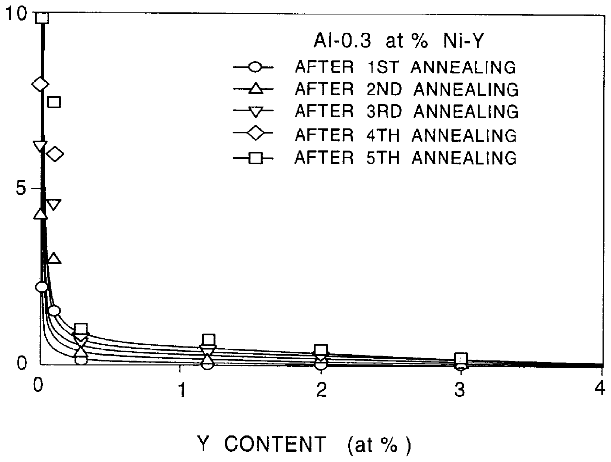
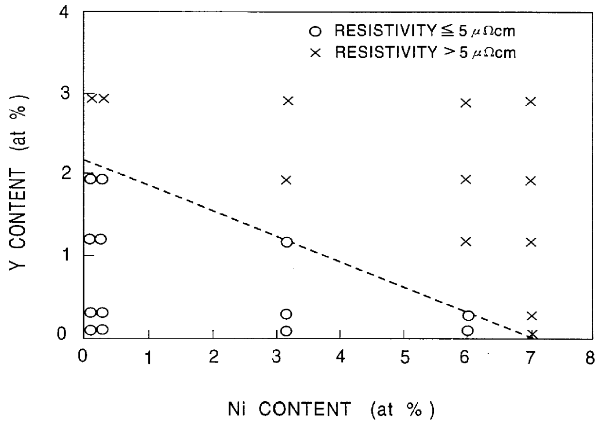
Alloy films with a thickness of 350 nm and having various compositions of Al-x at % Ni-y at % Y (x=0.1 to 7 and y=0.1 to 3) were deposited on substrates made of Corning No. 7059 glass with a thickness of 0.5 mm and a diameter of 50 mm by means of a DC magnetron sputtering using vacuum melted Al--Ni--Y alloy targets containing proper amounts of Ni and Y. The composition of the obtained Al--Ni--Y alloy films was analyzed by ICP. Then the films were patterned into a resistivity test pattern with a length of 10 mm and a width of 100 .mu.m by means of a wet etching process (using a mixed solution of H.sub.3 PO.sub.4 : HNO.sub.3 : H.sub.2 O=75: 5: 20 as an etchant) in conjunction with photolithography. The films were then subjected to a annealing at a constant temperature of 300.degree. C. for 0.5 hr in a vacuum ambient (at a pressure lower than 2.0.times.10.sup.-6 Torr) using a hot-wall furnace. After annealing, the resistivity of the thin films was measured using the four-...

embodiment 2

[Embodiment 2]

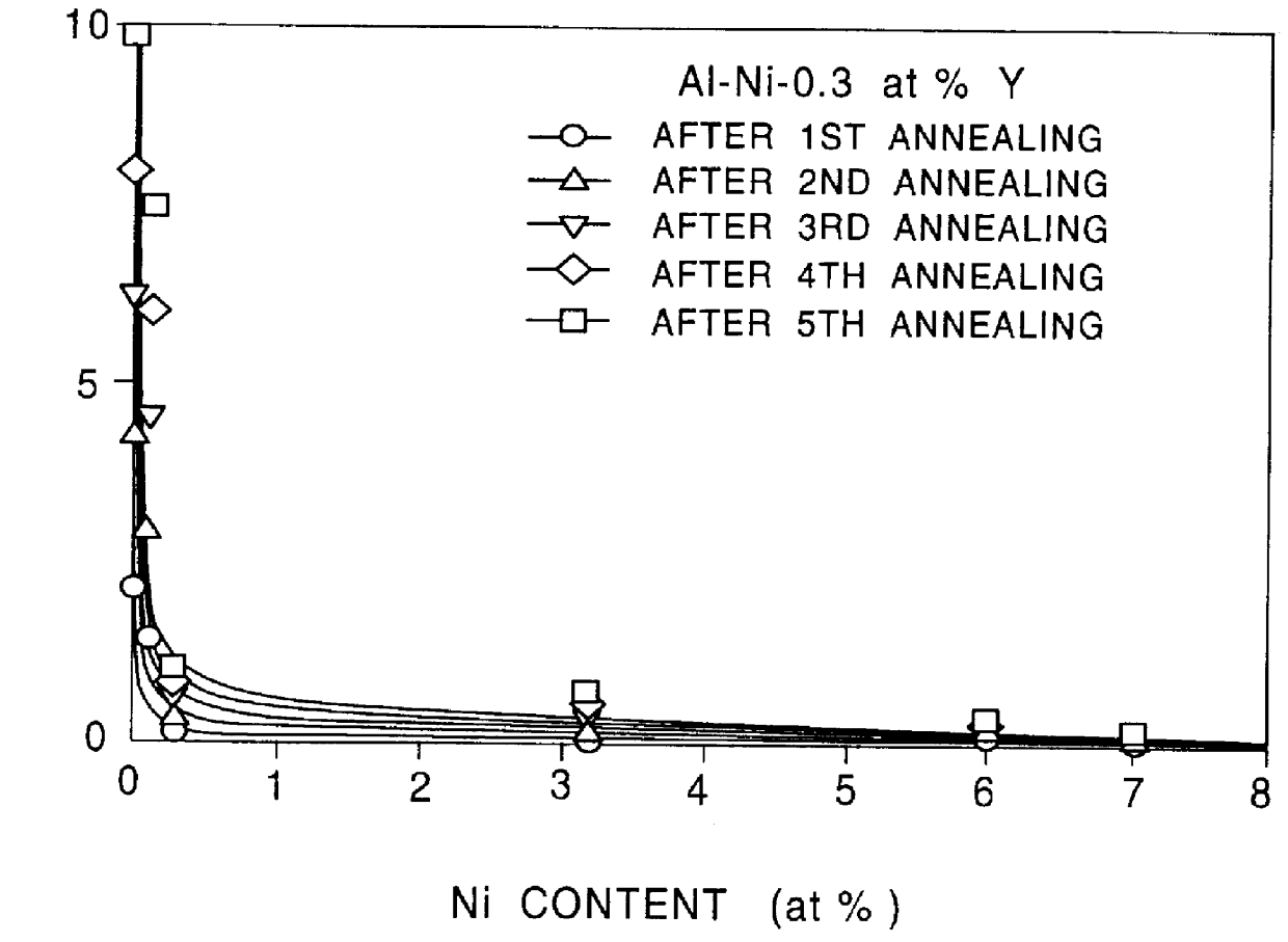
Alloy films with a thickness of 350 nm and having various compositions Al-x at % Ni-0.3 at % Y (x=0.1 to 7) were deposited on substrates made of Corning No. 7059 glass with a thickness of 0.5 mm and a diameter of 50 mm by DC magnetron sputtering using vacuum melted Al--Ni--Y alloy targets containing proper amounts of Ni and Y. The composition of the obtained Al--Ni--Y alloy films was analyzed by ICP. Then the films were patterned into a resistivity test pattern with a a width of 10 .mu.m by means of a wet etching process (using a mixed solution of H.sub.3 PO.sub.4 : HNO.sub.3 : H.sub.2 O=75: 5: 20 as an etchant) in conjunction with photolithography. The films were then subjected repeatedly (5 times) to an annealing at a constant temperature of 300.degree. C. for 0.5 hr in a vacuum ambient (at a pressure lower than 2.0.times.10.sup.-6 Torr) using the hot-wall furnace. The surface of the obtained thin films was observed under a microscope, and the hillocks density (the n...

embodiment 3

[Embodiment 3]

Alloy films with a thickness of 350 nm and having compositions of Al-2.0 at % Ni-1.5 at % Y, Al-1.6 at % Sc, and Al-1.0 at % La were deposited on substrates made of Corning No. 7059 glass with a thickness of 0.5 mm and a diameter of 50 mm by DC magnetron sputtering using Al--Ni--Y alloy targets containing proper amounts of Ni and Y according to the invention and also Al--Sc and of Al--La alloy targets as reference standards. The composition of the obtained Al alloy films was analyzed by ICP. The n the films were patterned into a resistivity test pattern with a width of 10 .mu.m by means of a wet etching process (using a mixed solution of H.sub.3 PO.sub.4 : HNO.sub.3 : H.sub.2 O=75: 5: 20 as an etchant) in conjunction with photolithography. The films were then subjected repeatedly (5 times) to an annealing at a constant temperature of 300.degree. C. for 0.5 hr in a vacuum ambient (at a pressure lower than 2.0.times.10.sup.-6 Torr) using the hot-wall furnace. The surface...


PUM

PropertyMeasurementUnit
thicknessaaaaaaaaaa
grain sizesaaaaaaaaaa
temperatureaaaaaaaaaa

Abstract

The invention provides an Al alloy film for use as an electrode of a semiconductor device and also provides an Al alloy sputtering target used to produce such an Al alloy film wherein the Al alloy film has not only a low resistivity equal to or less than 5 mu OMEGA cm and a high hillock resistance (property of hillock suppression) but also a high dielectric strength when it is anodized into an anodic oxide film and wherein the Al alloy film has a composition such that the Ni content is equal to or greater than 0.3 at % and the Y content is equal to or greater than 0.3 at % and such that 0.22 CNi+0.74 CY<1.6 at % where CNi denotes the Ni content (at %) and CY denotes the Y content (at %) and further wherein, in order to deposit the Al alloy film by sputtering, a spray forming Al alloy target containing Ni and Y is used.

Description

1. Field of the InventionThe present invention relates to an Al--Ni--Y alloy thin film for use as electrode of semiconductor devices and to an Al--Ni--Y alloy target used to produce such an Al--Ni--Y alloy thin film. More particularly, the present invention relates to an Al--Ni--Y alloy film particularly suitable for forming electrodes (electrodes themselves and thin film interconnections) in an active matrix liquid crystal display and to a sputtering target used to produce such Al--Ni--Y alloy films.2. Description of the Related ArtLiquid crystal displays (hereinafter referred to simply as LCDS) have the advantage of being smaller in thickness, being lighter in weight, and consuming less electric power than a conventional CRT display, and still being capable of displaying a high-resolution image. Liquid crystal displays are now widely used in many applications such as television sets and notebook-type personal computers. To improve the image quality such as resolution and contrast,...

Claims


Application Information

Patent Timeline
Patent Type & Authority Patents(United States)
IPC IPC(8): C23C14/34C25D11/04H01L23/52H01L23/532G02F1/1343C23C14/14H01L21/28H01L21/285
CPCC23C14/3414C25D11/04H01L23/53219H01L2924/0002H01L2924/00H01L21/285
Inventor TAKAGI, KATSUTOSHIONISHI, TAKASHI
Owner KOBE STEEL LTD
Why Eureka
Try Eureka